
Ā
Ā
A Classic PLL block diagram
Fuding Ge
Introduction
A phase-locked loop is a sort of circuit whose output signal keep a
constant phase difference with a reference signalĀ through feedback.
It can be described using the following diagram:
Now look at the classic PLL block diagram as shown blow:
Ā
Ā
Ā
Ā
A Classic PLL block diagram
Here the frequency of the output signal Vout, fout, is related to the frequency of the reference signal Vref, fref,Ā by the following equation:
fout = Nfref = f0 + VcKvco
where f0 is the free running frequency of the VCO and Kvco is the VCO conversion gain.
Some basic concepts about PLL
Now let have a look at some basic concepts that characterize a PLL
system.
Free running frequency is the VCO output frequency when the PLL is not in lock or the there is no input signal.
Hold-in range (Hold range, Lock range):Ā It is the static
stability limit. When the PLL is in the phase-locked state, the maximum
frequency range in which the frequency of the input reference signal can
slowly be pulled away from the
free running frequency of the VCO but the PLL still maintain the phase-locked
condition is called the hold-in range.
Lock-in range (Pull-in range, Capture range): It refers to the condition that initially the PLL is not in the phase-locked state, then the reference input signalĀ frequency slowly approaches the free running frequency of the VCO, the maximumĀ frequency range in which the input signal eventually becomes phase-locked is called the lock-in range or capture range.
Pull-out range: It is the dynamic stability limit of the PLL. It is the maximum value of a frequency step that apply to the input reference signal of a phase locked PLL and the PLL still maintains the lock state. If the frequency step exceeds the pull-out range, the PLL will not be able to track the input signal and fall out lock. The PLL may acquire lock again through a slow pull in process.
Lock range: This range is a subset of pull-in range, It is the range that the PLL will acquire lock within a single beat between the input reference signal and the feedback signal.
Lock-up time (Acquisition time): The amount of time required for the loop to phase lock is called lock-up time or acquisition time.
Phase noise (Time Jitter)
Phase Detector Dead Zone
Cycle Duty
Ā
Ā
Ā
Feedback control system
First let's look at a generalized feedback control system, as shown
in the following figure:
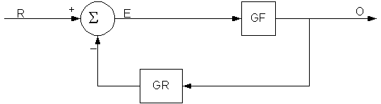
Block diagram of a feedback control system
GF is the forward gain and GR is the gain of feedback loop. R is the reference signal, E is the error signal and O is the output signal of the closed loop system. We have
O/R = GF / (1+GF*GR)
E/R =ĀĀ 1 /Ā (1+GF*GR)
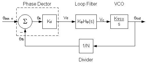
PLL linear model
A generalized PLL linear model is shown in the following figure:

PLL Linear Model
Compare this model with the feedback control system, we find that:
and the phase transfer function of the PLL is:GF = KdKlpHlp(s)Kvco/s
GR = 1/N
H(s) = qout/qref = GF/(1+GF*GR) = (KdKlpHlp(s)Kvco)/(s+KdKlpHlp(s)Kvco/N)
Now define the loop gain
H(s)Ā = NG/(1+G)
The phase error transfer function is:
qe/qref =1/(1+GF*GR) =s/(s+KdKlpHlp(s)Kvco/N)
Noise analysis based on linear model
The input noise transfer blocks can be modeled as following:
Hinn = NG/(1+G)
The transfer of low pass filter noise is modeled as following:
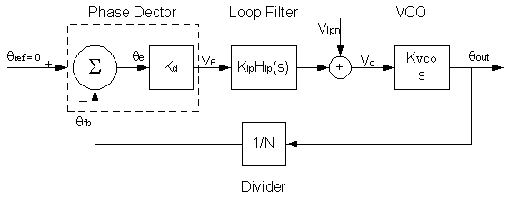
GF = Kvco/s
GR = KdKlpHlp(s)/N
So the transfer function of low pass filter noise Vlpn is
Hlpn(s) = qout/Vlpn = GF/(1+GF*GR) = (Kvco/s)/[(1+KvcoKdKlpHlp(s)/(sN)] = Kvco/[s+KvcoKdKlpHlp(s)/N]
The transfer of VCO noise is modeled as following:
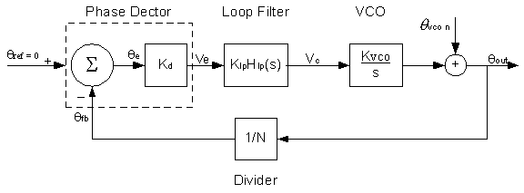
The transfer function is:
Hvcon = 1/(1+G)
Practical PLL Design
The most practical and popular phase detector and loop filter are shown in the following figure. It consists of a charge pump phase frequency detector (PFD) which supply current to loop filter. The filter converts the charge pump error current into the VCO control voltage.
Normally the value of C2 is much smaller than C1 (about 0.1C1), then
for a first order analysis, C2 can be neglected.
Ā
Ā

If this is true, we have:
Kd = I/(2p) (A/Radian)
KlpH(s) = R+1/(sC1)
Substitute Kd and KlpH(s) into the phase transfer function of PLL, we have:
![]()
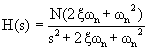
From this equation we can find that this is a typical second order system. (In fact as a general rule, if the order of the loop filter is M, then the order of the PLL is M+1.) The nature frequency of the system is:
![]()
and the damping factor of the system is:
Then H(s) can be written in a more general form:
The switching interaction between the charge pump and the loop filter causes a great deal of ripple on the VCO control voltage with the series RC loop filter (in the figure it is RC1). This ripple can be suppressed by adding the small capacitor, C2, in parallel with the RC loop filter as shown in the figure.
The addition of C2 adds another pole to the PLL transfer function and makes it a 3rd order system. However, if the capacitor is smaller enough the system can be treated as a 2nd order system (C2<0.1C1).
The function of phase detector and loop filter is to provide a DC voltage proportional to the phase difference which is then used to control the frequency ofĀ VCO.Ā The charge pump system is actually a discrete time system. The above continuous time linear analysis holds only when the input reference frequency is significantly larger than the loop nature frequency wn.ĀĀ The loop bandwidth is closely related to wn and a formal stability limit is given:
wn2< wref2Ā /p(RC1wn+p)
If Kvco and I is known, using the above equations, the values of the loop filter components R, C1 and C2 can be determined.
Here is a dynamic program for low pass filter design for PLL
 visitor to this page.