 |
||||||||||||||||||||||||||||||||||||||||||||||
ISA-24-IO Connection
Feature
Schematic
Note
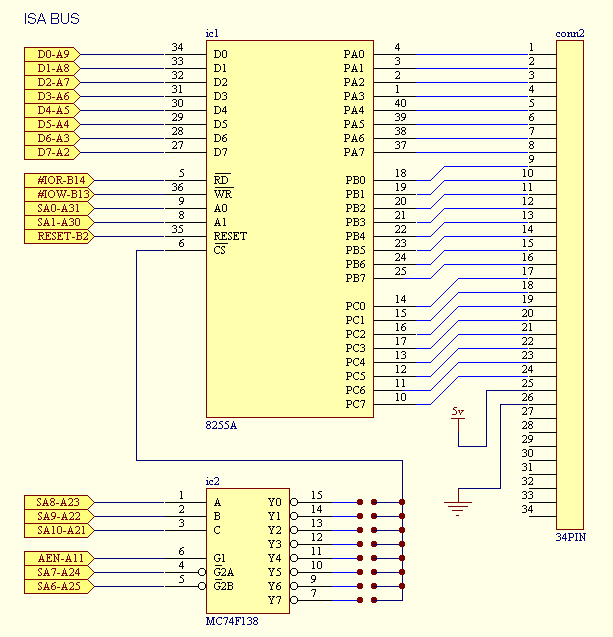
Function The card is very simple. The 8255 does most of the job interfacing data and control lines from the ISA, in fact they are connected directly. The three 8bit IO ports are controlled via the 8255 through the ISA connection. The rest is the address decoding part. The only address pins used are SA0 to SA10. A1 and A0 are used directly for 8255 internal addressing. The address range usable by the card uses is 0x300-0x33f and 0x340-0x37f, since this range is free for expansion and does not conflict with other normal PC resources.
Note that SA19 to SA11 are unusable in an PC-XT.
Therefore the address decoder chip (74LS138) has to use the pins as showed above, and with this data control the 8255 chip. The 74LS138 has 3 selector pins (A,B,C) which control which of the 8 outputs is to be pulled low. It also has 3 enable pins called G1, G2A, and G2B. For one of the outputs to be pulled low G1=1, G2A=0 and G2B=0. Therefore the pins are connected as shown
74ls138 pinouts A----A8---1
Programming Programming is easy, now that you have calculated you base address, all you need to know is the address of the three 8255 registers and the 8255 control register.
base_address=0x300; outp(base_address+3,0x80); // put all registers as output outp(base_address,0x255); // pull all register A up outp(base_address+1,0x255); // pull all register B up
Interfacing The 8255 method of interfacing should be found on the datasheet itself. The 8255 are supposed to be TTL and CMOS compatible. For unpredictable loads you should place some kind of isolator between the chip and the load, to protect the card (and the PC) from surges, short-circuits, etc.. To use with heavy loads you should buffer your output using some transistors or a suitable chip would be an ULN2803A. Note that the length of the ribbon cable between the connector and the outside must be of a limited length. I have encountered some problems with lengths greater than 0.5metres.
Expansion The card could be easily upgraded from 24bit to 48bit,96bit. However the space available on the board will limit the number of 8255 you can place on the board. By improving the address decoding, you can use the multiple outputs available from the address decoder to select different 8255s. As you can see in the schematic of ISA-24-IO address lines SA2 to SA5 are not used anywhere in the address decoding. By using these four lines in a multiplexer. (3 to 8 or 4 to 16 multiplexer can easily be found). Each of the multiplexor output would be fed into the CS (pin 6) of each 8255. Note that the output from the address decoder 74ls138 would be connected to the multiplexor and not to the 8255. The data D0 to D7, control lines IOR,IOW, RESET and addresses SA0 to SA1 would be the same for all 8255s. Now the address decodes addresses for example 0x300 - 0x302 : first 8255 0x303 - 0x304 : second 8255 and so on Here is a pdf file of the schematic 4 or more 8255s on one ISA card Do not forget to decouple your ICs with suitable capacitors. I will issue PCB masks soon I am just waiting to set up the CNC machine. If you request more information mail me fishziblu. |
||||||||||||||||||||||||||||||||||||||||||||||