The old version is the version I did with Larry McDaniel.
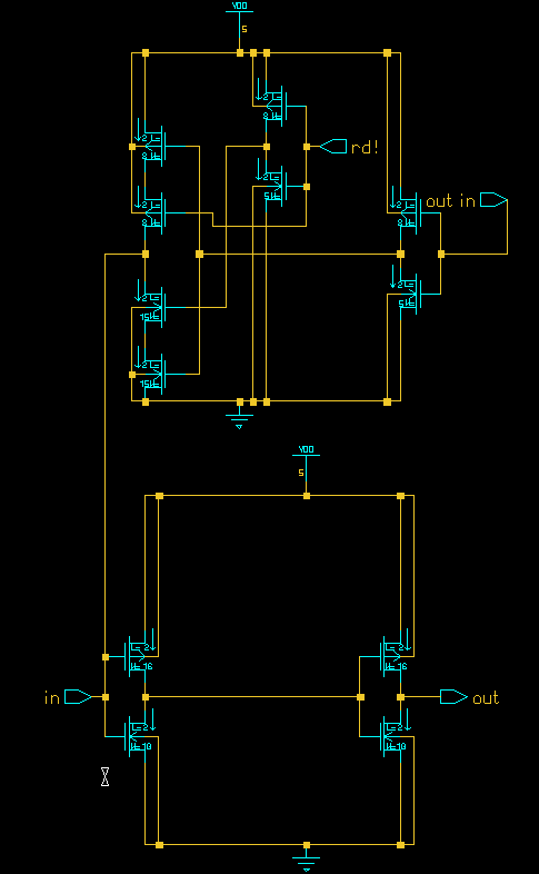
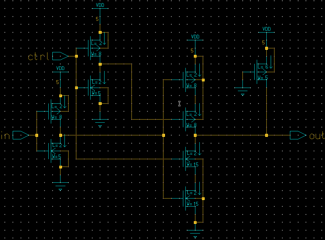
The Memory Interface (MI) was responsible for loading to and from the bus from the memory that is off the chip. It is a simplified part with just two tri-state gates to load data from the bus with an invertering control signal. To minimize the part the pad was used as one tristate and a buffer was used in the part (MI cell in DA)(MI cell in IC Station). The simulation results were in both Accusim and MachTA.
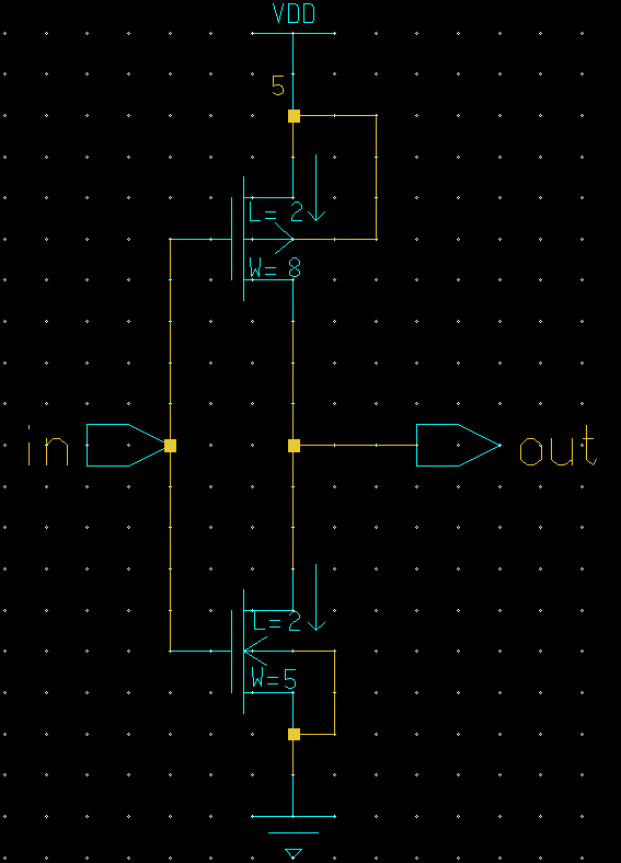
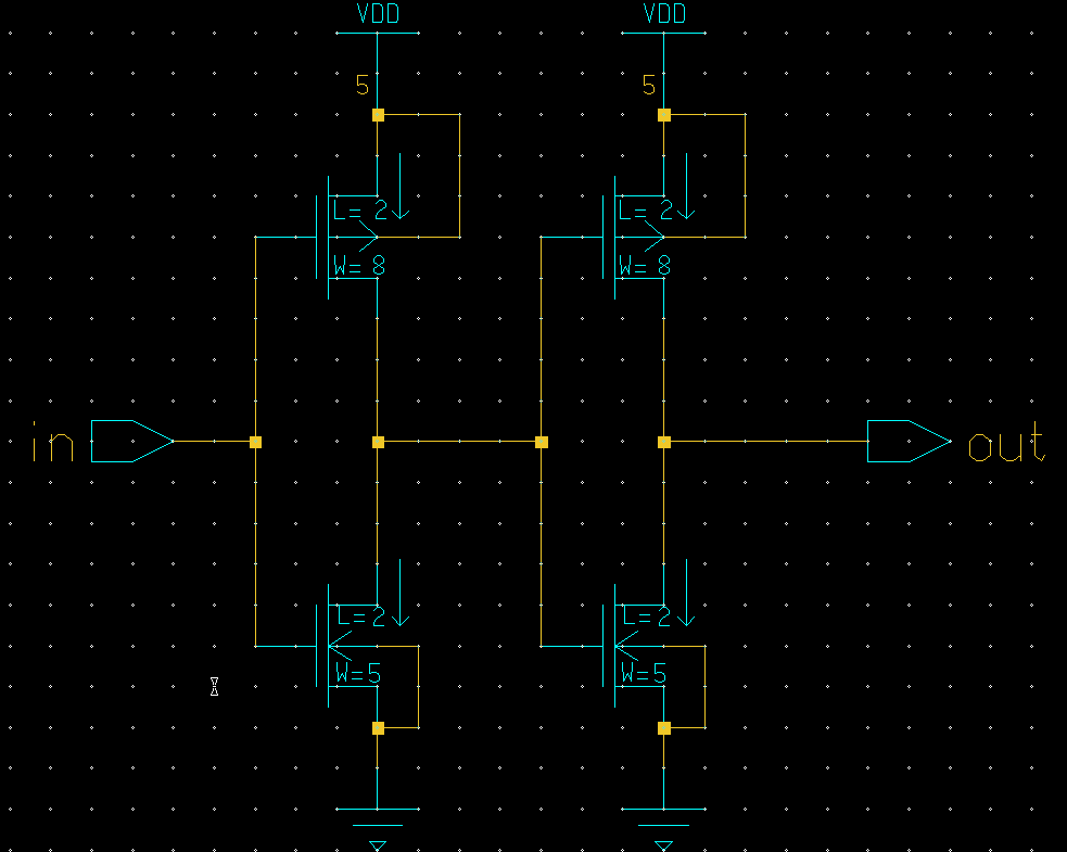
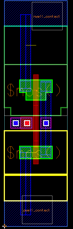
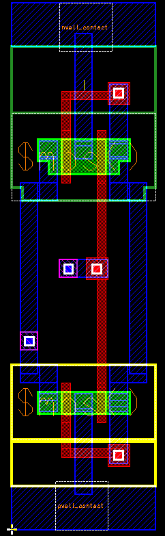
The memory Interface had several other parts as well. The Design Architect (DA) of these parts are INVERTER and the BUFFER. The IC Station of these parts in there CMOS old form is INVERTER IC and BUFFER_IC.
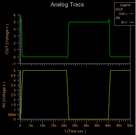
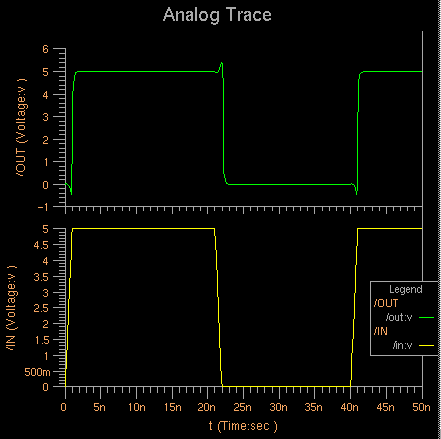
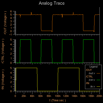
The Accusim simulation results: INVERTER, BUFFER. The MachTA simulation results: INVERTER, BUFFER.
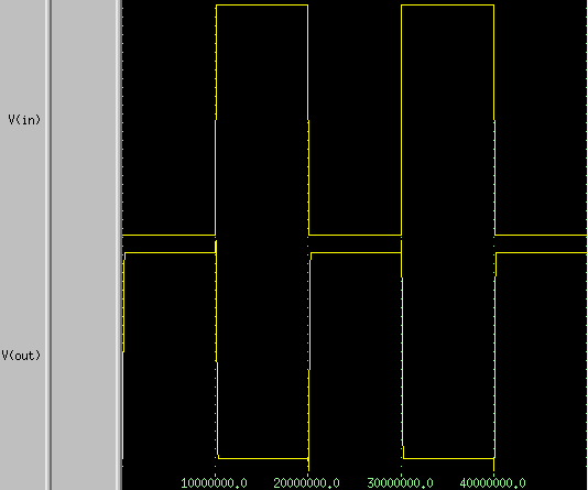
All of these parts together act as the MI (OLD MI). The simulation in Accusim of the MI is in parts: Part 1, Part 2, Part 3, Part 4, Part 5, and Part 6. The cells of these parts were placed together to form the MI (OLD MI IC)(OLD MI peeked).
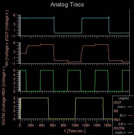
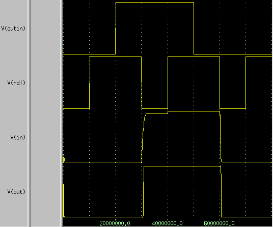
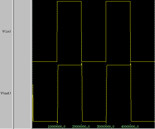
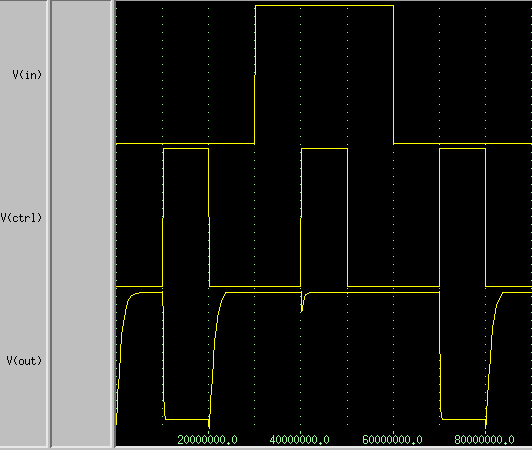
Then we had to test the parts with a DO File and a Test Vector File. The simulation results are here: Part 1, Part 2, Part 3.
This version I did myself over Christmas 2000. Due to time restrictions we were unable to assemble the chip during the class. So a second class was added to assemble the parts.
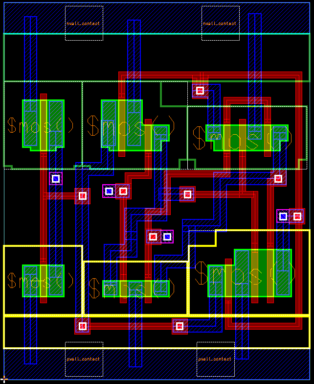
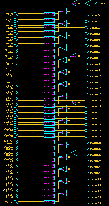
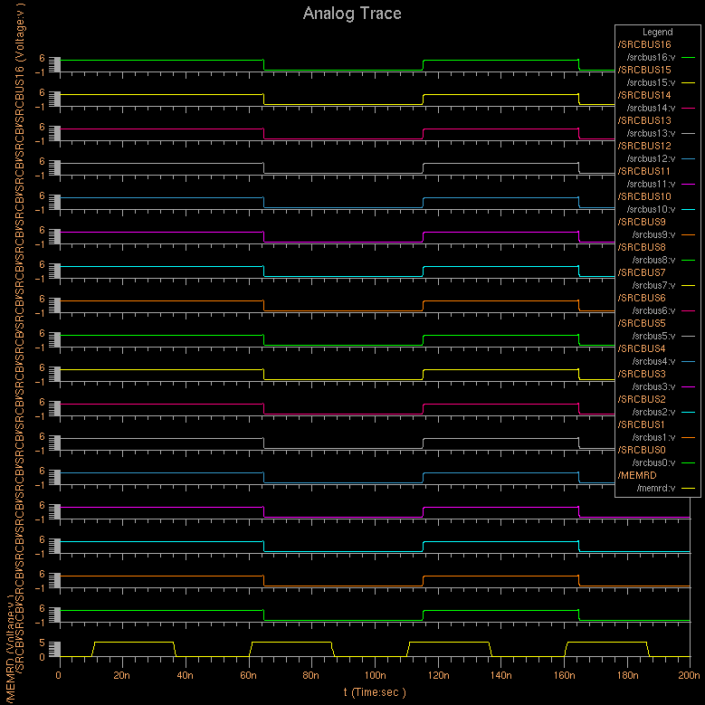
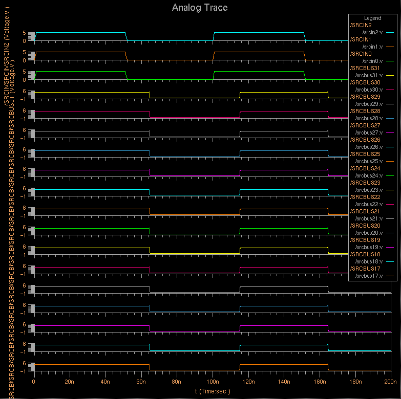
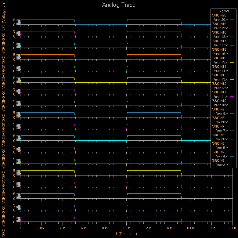
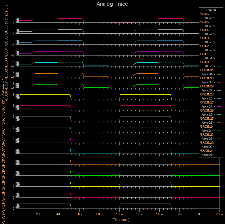
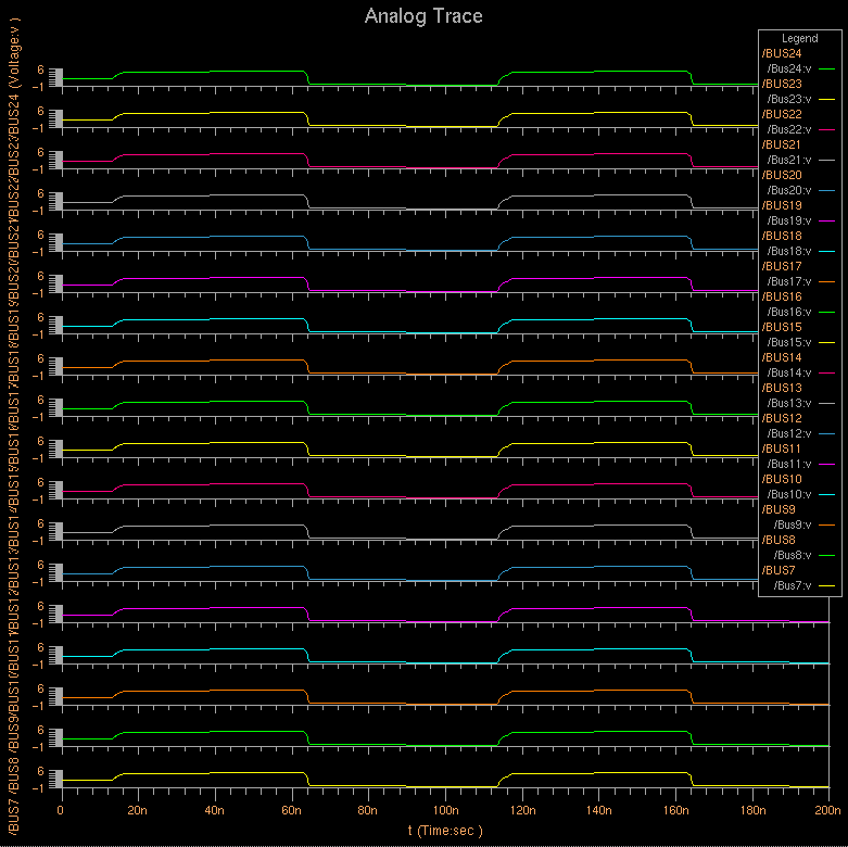
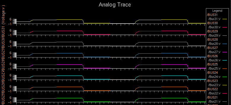
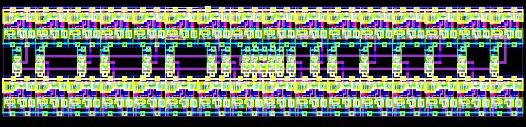
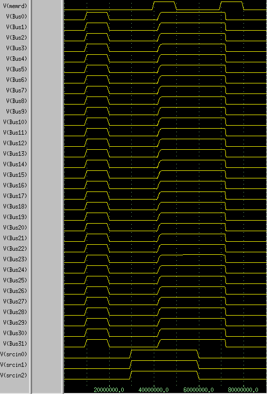
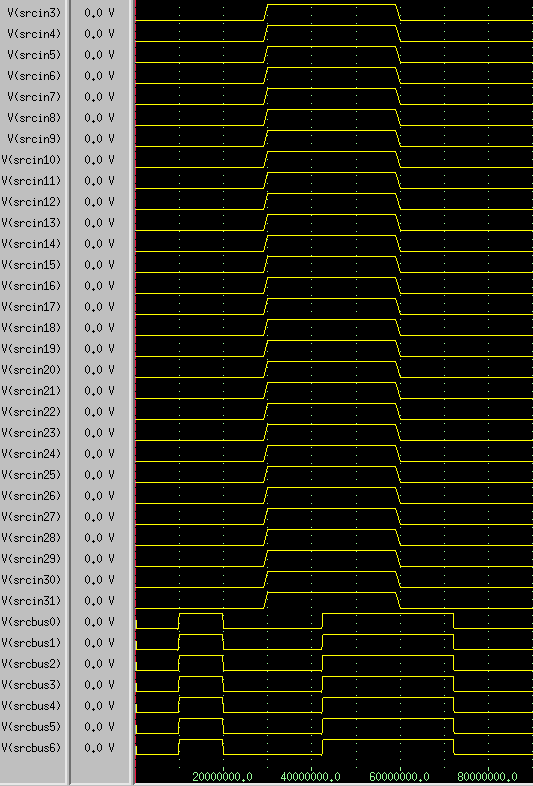
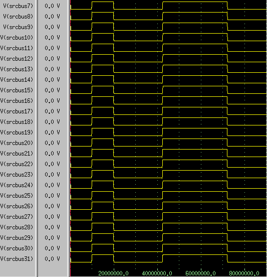
The MI component was re-done in DA to include the pull-up for the bus. The simulation result is here. To make the MI smaller to save space on the chip I broke it into 32 individual components and placed by each corresponding pad. They are the same as the old IC Station cells of the MI but stretched to allow easy connection to the pads and the bus lines are now pull-up to prevent the bus from floating during idle cycles. The MachTA simulation is here.
There were no other parts needed. The Testing was just to test the individual part, no dofile was needed.