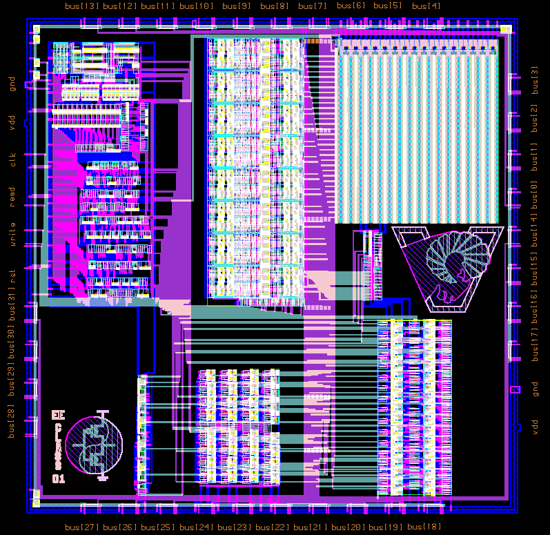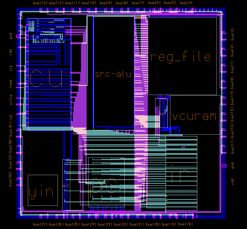
The chip assembled my parts (Memory Interface and Instruction Register) and other peoples parts. They were all placed in a layout of a the pad and tested. Below are 2 pictures of the schematic, click to see larger version.
I wired the Register File, IR, MI, Condition Control Logic (CCL), and ALU to the bus I drew down the center-right side as well as to power and ground. My IR is in the lower right corner, and the MI is next to the bus pads around the chip on the inside of the power and ground rails.
To go to the main webpage of the SRC II Chip click here.