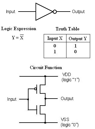
The standard CMOS inverter consists of one p-type transistor connected to the power rail joined at the inverter output to one n-type connected to the ground with rail with their common gates connected to the inverter input.
p-type is always used to make output logic "1" (VDD)
n-type is always used to make output logic "0" (VSS)
The key to full voltage levels of the CMOS inverter output is that the output is a drain of both of the transistors.
If there is 0V on the input to this inverter, the p-type is switched ON and the n-type is switched OFF; thus, there is a connection between the power rail and the output, and so charge flows onto the output. If there is 5V on the input, the p-type is OFF and n-type is ON; any charge on the output flows through the channel in the n-type to the ground rail. A HIGH voltage on the input leads to a LOW voltage on the output; a LOW voltage on the input leads to a HIGH voltage on the output: we have an electrical implementation of NOT gate. |