![]()
![]()
![]()
LATCH Circuits
or circuits with a MEMORY
There are often two outputs shown from the latch. One is defined as the opposite of the other. They are shown here as Q and “Q bar”.
If these two outputs are the same then this is a state that cannot be allowed and is sometimes called forbidden. If you create a circuit that breaks the rule then you will also create errors in other circuits that are connected.
This is a NOR RS LATCH
Its forbidden state is when R and S are 1.
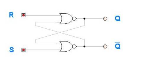
The memory state is when R and S are 0.
|
R |
S |
Q |
notQ |
|
|
|
0 |
0 |
No change |
Memory |
|
|
|
0 |
1 |
1 |
0 |
|
|
|
1 |
0 |
0 |
1 |
|
|
|
1 |
1 |
0 |
0 |
This is forbidden |
|
The timing diagram starts off with the memory state. As we don’t know what it was before this state we can’t work it out. This is why the ? is used.
The forbidden state is shaded in yellow.
The states of R and S are random.
|
nor RS latch |
|
|
|
|
|
|
|
|
|
|
|
S |
|
|
|
|
|
|
|
|
|
|
|
|
|
|
|
|
|
|
|
|
|
|
|
R |
|
|
|
|
|
|
|
|
|
|
|
|
|
|
|
|
|
|
|
|
|
|
|
Q |
? |
|
|
|
|
|
|
|
|
|
|
|
|
|
|
|
|
|
|
|
|
|
|
not Q |
? |
|
|
|
|
|
|
|
|
|
|
|
|
|
|
|
|
|
|
|
|
|
This is a NAND RS LATCH
Its forbidden state is when R and S are 0.

The memory state is when R and S are 1.
|
R |
S |
Q |
notQ |
|
|
|
0 |
0 |
1 |
1 |
This is forbidden |
|
|
0 |
1 |
1 |
0 |
|
|
|
1 |
0 |
0 |
1 |
|
|
|
1 |
1 |
No change |
Memory |
|
|
|
nand RS latch |
|
|
|
|
|
|
|
|
|
|
|
S |
|
|
|
|
|
|
|
|
|
|
|
|
|
|
|
|
|
|
|
|
|
|
|
R |
|
|
|
|
|
|
|
|
|
|
|
|
|
|
|
|
|
|
|
|
|
|
|
Q |
|
|
|
|
|
|
|
|
|
|
|
|
|
|
|
|
|
|
|
|
|
|
|
not Q |
|
|
|
|
|
|
|
|
|
|
|
|
|
|
|
|
|
|
|
|
|
|
![]()
![]()
![]()