 History
Introduction
Overview of the FPGA construction
The
FPGA
History
With
the introduction of the Field Programmable Gate Array (FPGA
- a configurable- logic chip) in the early 80s, the hardware engineer
was empowered to implement chip-level designs in silicon without having
to fabricate a chip. As these devices and their software tools matured,
the use of FPGAs expanded from testing and verifying digital designs
to in-system use. This overview describes the fundamentals as well
as current uses of this technology.
FPGAs
perform the function of a custom LSI circuit, like a gate array, and
are user programmable. The most significant advantage of using FPGA
devices is the ability to produce a prototype logic design, implementing
it in silicon within hours, while conventional gate array devices
can take months and many dollars to develop and produce working silicon.
Since their introduction, FPGAs have continued to increase in useable
gate count, while decreasing in price. They are currently being used
as glue logic, for test / verification logic in system designs, for
adaptable system designs and more recently as coprocessing devices.
FPGAs are also used to emulate other component architectures, and
are applicable for rapid prototyping. With the next generation of
SRAM based FPGAs (designed with computing in mind) a whole new generation
of computing applications will result.
Introduction
The Field
Programmable Gate Array or FPGA as it is more widely called is a type
of programmable device. Programmable devices are a class of general-purpose
chips that can be configured for a wide variety of applications. The
first programmable device which achieved a widespread use was the
PROM (Programmable Read-Only Memory). PROMs, a one-time programmable
device come in two basic versions: 1) The Mask-Programmable Chip programmed
only by the manufacturer, 2) The Field-Programmable Chip programmed
by the end-user. The Field Programmable PROM developed into two types,
the Erasable Programmable Read-Only Memory (EPROM) and the Electrically
Erasable Programmable Read-Only Memory (EEPROM). The EEPROM has the
advantage of being erasable and reprogrammable many times.
Another
step took place in this field which lead to the development of the
Programmable Logic Device (PLD). These devices were constructed to
implement logic circuits. The PLD included an array AND gates connect
to an array of OR gates. The PAL (Programmable Array Logic) is a commonly
used PLD consisting of a programmable AND-plane followed by a fixed
OR-plane. PALs come in both mask and field versions. The PAL was designed
for small logic circuits.
The Mask-Programmable
Gate Array (MPGA) was developed to handled larger logic circuits.
A common MPGA consists of rows of transistors that can be interconnected
to implement desired logic circuits. User specified connects are available
both within the rows and between the rows. This enabled implementation
of basic logic gates and the ability to interconnect the gates. As
the metal layers are defined at the manufacturer, significant time
and cost are incured in producing the run. In 1985, Xilinx Inc. introduced
the FPGA (Field Programmable Gate Array). The interconnects between
all the elements were designed to be user programmable.
Overview
of the FPGA construction
There
are four main categories of FPGAs currently commerically available:
symmetrical array, row-based, hierarchical PLD, and sea-of-gates
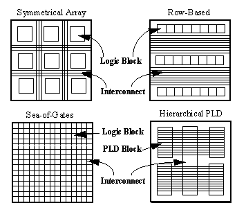
Figure
1: Classes of FPGA
In
all of these FPGAs the interconnections and how they are programmed
vary. Currently there are four technologies in use. They are: static
RAM cells, anti-fuse, EPROM transistors, and EEPROM transistors.
Static
RAM Technology -- In the Static RAM FPGA programmable connections
are made using pass=transistors, transmission gates, or multiplexers
that are controlled by SRAM cells. The advantage of this technology
is that it allows fast in-circuit reconfiguration. The major disadvantage
is the size of the chip required by the RAM technology.
Anti-Fuse
Technology -- An anti-fuse resides in a high-impedance state; and
can be programmed into low impedance or "fused" state. A less expensive
than the RAM technology, this device is a program once device.
EPROM
/ EEPROM Technology -- This method is the same as used in the EPROM
memories. One advantage of this technology is that it can be reprogrammed
without external storage of configuration; though the EPROM transistors
cannot be re-programmed in-circuit. The following table shows some
of the characteristics of the above programming technologies.
The
FPGA
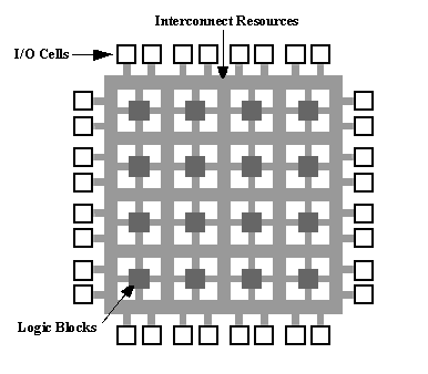
Figure
2: The FPGA structure
The
FPGA has three major configurable elements: configurable logic blocks
(CLBs), input/output blocks, and interconnects. The CLBs provide the
functional elements for constructing user's logic (Figure 2). The
IOBs provide the interface between the package pins and internal signal
lines. The programmable interconnect resources provide routing paths
to connect the inputs and outputs of the CLBs and IOBs onto the appropriate
networks. Customized configuration is established by programming internal
static memory cells that determine the logic functions and internal
connections implemented in the FPGA.
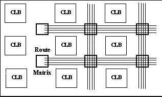
Figure
3: CLBs interconnect
Figure
3 depicts a FPGA with a two-dimensional array of logic blocks that
can be interconnected by interconnect wires. All internal connections
are composed of metal segments with programmable switching points
to implement the desired routing. An abundance of different routing
resources is provided to acheive efficient automated routing. There
are four main types of interconnect, three are distinguished by the
relative length of their segments: single-length lines, double-length
lines and longlines. (NOTE: The number of routing channels shown in
the figure are for illustration purposes only; the actual number of
routing channels varies with the array size.) In addition, eight global
buffers drive fast, low-skew nets most often used for clocks or global
control signals.
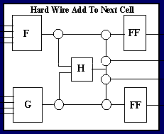
Figure
4: Configurable Logic Blocks
The
principle CLB (Configurable Logic Block) elements are shown in Figure
4. Each CLB contains a pair of flip-flops and two independent 4-input
function generators. These function generators have a good deal of
flexabilty as most combinatorial logic functions need less than four
inputs. Configurable Logic Blocks implement most of the logic in an
FPGA. The flexabilty and symmetry of the CLB architecture facilitates
the placement and routing of a given application.