Combinational Design with Multiplexers and Demultiplexers
Jared L. Crum
Department of Electrical & Computer Engineering
Youngstown State University
E-mail: [email protected]
ABSTRACT: The 74153 dual 4-1 multiplexer is used to send four signals
through one data line. The 74155 dual
1-4 demultiplexer is used to take this data and send it back to four separate
lines. Experimental results from
testing a circuit in which a 4-1 multiplexer is connected to a 1-4
demultiplexer are compiled. These
results make it easy to
see that the compliment of the selected input is the value of the selected
output, and the rest of the outputs are 1. This method of sending several
signals through one line is useful in reducing the wires needed to send data
over long distances. However, since two
select lines must be used in addition to the data line, this method is not
practical unless more signals are sent through one line. Therefore, a design for sending eight signals
through one data line is presented.
This design uses these two chips, three select lines, one OR gate, two
inverters, and one data line.
1. Introduction
A multiplexer is a digital circuit that will channel one of several data inputs to its output depending on that status of select inputs. A demultiplexer, on the other hand, takes one data input and transfers it to one of several outputs depending on the status of the select inputs. For more information on multiplexers and demultiplexers see section 5.7 of Digital Design by Wakerly [1]. Specifically, the 74153 dual 4-line to 1-line multiplexer, and the 74155 1-line to 4-line decoder/demultiplexer will be considered. The specifications for these chips can be found on spec sheets published by the National Semiconductor Corporation [2,3].
The 74153 chip has two multiplexers that each transfer a value from one of their four inputs to their output. Hence, it is called a dual 4-line to 1-line multiplexer. However, since both multiplexers on this chip share the same set of select inputs they must be used as a pair. They cannot be used in two separate applications simultaneously, but they can be combined to form 8-line to2-line multiplexer. Therefore, it would be more appropriate to call it a two-bit 4-line to 1-line multiplexer than to call it a "dual" multiplexer. Similarly it would be more appropriate to call the 74155 demultiplexer a two-bit demultiplexer since both demultiplexers on the chip share the same select inputs. This 74155 chip acts as a decoder 2 to 4 when its data input is held to a high voltage. Therefore, it is called a decoder/demultiplexer. A decoder is a device that sends a signal to an output corresponding to its binary input. In this case, the two select lines can act as the inputs. Though the decoder is a fascinating device, the demultiplexing capabilities of the 74155 chip will be primarily considered. Diagrams of both the 74153 chip and the 74155 chip are shown in figure 1. This figure also shows how these chips are hooked up in a circuit that will be discussed latter.
The output of the 74153 multiplexer is considered active-1. This means that its output will be low unless it is activated, in which case it will be high. From the diagram it is easy to see that it is active-1 since it does not have a bubble on the output or a bar above its label. The input lines and select lines of the multiplexer are also active-1. Pins 1 and 15 are the enable inputs, meaning that they can either enable or disable the respective multiplexer. The enable inputs, which can also be called strobe inputs, allow the multiplexer to function if and only if this input is active. Since the enable inputs are active 0, the multiplexer will be disabled unless the enable input has a value of 0. Interestingly, the diagram for this input is incorrect. The diagram shows both a bubble and a bar on this input. Since two negatives make a positive this is an incorrect diagram.
The outputs of the 74155 demultiplexer are active 0. This means that its output will be high unless it is activated, in which case it will be low. Pins 1 and 15 are the inputs of the two demultiplexers on the 74155 chip, and these inputs are active 1. Pins 2 and 14 are the enable inputs of the multiplexer, and they are active-0. Interestingly, the diagram representations of these inputs are correct since they only use bars without bubbles. However, it seems that the bubble representation is preferable since the bar can easily be missed.
An experiment was conducted in which the output of the 4-1 multiplexer was tied to the input of the 1-4 demultiplexer. The circuit that was built is displayed in figure 1.
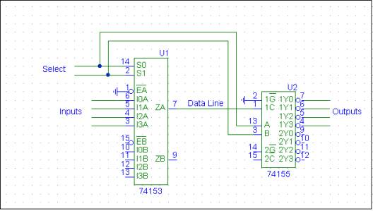
Figure 1: Experimental Circuit Using a 4-1 Multiplexer and a 1-4 Demultiplexer
2. Building a
Multiplexer to Demultiplexer Circuit
This circuit consisting of only two chips was built on the breadboard of the CADET II trainer unit. The CADET II trainer unit has many devices useful for circuit design and experimentation such as data input switches and logic output display lights. Using this unit the output of multiplexer was connected to the input of the demultiplexer. Also, the inputs of the multiplexer were connected to the logic switches, and the outputs of the demultiplexer were connected to the display lights.
Initial efforts to built the multiplexer to demultiplexer circuit failed. After studying the two chips it was realized that the enable inputs had to be connected to ground, and the circuit that resulted is shown in figure 1. By changing input values with the data switches and recording the logic outputs shown by the display lights, table 1 was compiled. Table 1 shows that the output of the demultiplexer is active-0 since output value is 1 unless it is activated by a selected input of 1. This table makes it easy to see that the compliment of the selected input is the value of the selected output and the rest of the outputs are 1.
Table
1: Results of Multiplexer to
Demultiplexer Circuit
|
Select |
Data Inputs |
Data Outputs |
|||||||
|
S0 |
S1 |
I0A |
I1A |
I2A |
I3A |
1Y0 |
1Y1 |
1Y2 |
1Y3 |
|
0 |
0 |
0 |
x |
x |
x |
1 |
1 |
1 |
1 |
|
0 |
0 |
1 |
x |
x |
x |
0 |
1 |
1 |
1 |
|
0 |
1 |
x |
0 |
x |
x |
1 |
1 |
1 |
1 |
|
0 |
1 |
x |
1 |
x |
x |
1 |
0 |
1 |
1 |
|
1 |
0 |
x |
x |
0 |
x |
1 |
1 |
1 |
1 |
|
1 |
0 |
x |
x |
1 |
x |
1 |
1 |
0 |
1 |
|
1 |
1 |
x |
x |
x |
0 |
1 |
1 |
1 |
1 |
|
1 |
1 |
x |
x |
x |
1 |
1 |
1 |
1 |
0 |
Table 2 is useful in showing more clearly the transmission of the data since most of the ones in outputs are not the result of data transmission. In table 2, "Â" is displayed in the output where data is actually being transmitted.
Table
2: Transmission of Data Made Clear
|
Select |
Data Inputs |
Data Outputs |
|||||||
|
S0 |
S1 |
I0A |
I1A |
I2A |
I3A |
1Y0 |
1Y1 |
1Y2 |
1Y3 |
|
0 |
0 |
A |
x |
x |
x |
 |
1 |
1 |
1 |
|
0 |
1 |
x |
A |
x |
x |
1 |
 |
1 |
1 |
|
1 |
0 |
x |
x |
A |
x |
1 |
1 |
 |
1 |
|
1 |
1 |
x |
x |
x |
A |
1 |
1 |
1 |
 |
3. Applications
of the Multiplexer to Demultiplexer Circuit
This circuit can be used to make the transmission of data over long distances easier. It can allow four signals to be transmitted with one data line and two select lines instead of four data lines. This does not seem to be that practical since it only saves on wire, but when more signals are sent through one data line it is practical. A method for sending eight signals through with only one data line and three select lines is discussed in the next section. First though, a method for addressing each data line in a systematic and orderly fashion will be discussed. Connecting a flip-flop circuit that repeatedly counts from zero to three to the select lines of both the multiplexer and the demultiplexer will systematically address four signals. For the transmission of eight signals the flip-flop circuit would need to count from zero to seven, and three select lines would be necessary.
4. The Design of an 8-1 Multiplexer to 1-8 Demultiplexer Circuit
A circuit using one 74153 chip, one 74155 chip, two inverters, and one OR gates is designed to transfer eight signals through one data line (a single 7402 NOR gate chip can supply two inverters and an OR gate). This design is shown in figure 2.
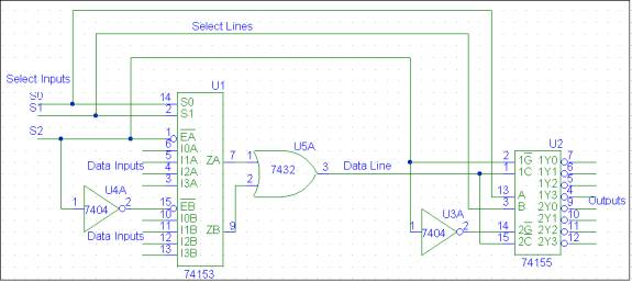
Figure 2: Circuit Design for Transmission of Eight
Signals Through One Data Line
Creating a third select line and connecting it to the enable inputs is the first step to building this circuit. An inverter is needed between the enable inputs so that one multiplexer is enabled while the other one is disabled, and likewise with the demultiplexers. Also, an OR gate was used to put both outputs of the multiplexer into one data line. This design can be useful in sending data through one line.
4.
Conclusion
The 74153 dual 4-line to 1-line multiplexer, and the 74155 1-line to 4-line encoder/demultiplexer are extremely useful tools for sending digital data over longer distances. The 74153 chip can be used to make either a 4-1 or a 8-1 multiplexer. Further, the 74155 can be used to make either a 1-4 or a 1-8 demultiplexer with active-0 outputs. By connecting one data line and the select input lines, a multiplexer to demultiplexer circuit can be constructed. One of these circuits was constructed and the results are shown in table 1. This table makes it easy to see that the compliment of the selected input is the value of the selected output and the rest of the outputs are 1. With just these two chips eight signals can sent through only one data line. This is useful for sending data over longer distances. After experimenting with these chips it is easy to see how practical their uses are.
References
[1] John
F. Wakerly, Digital Design: Principles and Practices—Third Edition Updated,
pp. 398-409, 2001
[2] National Semiconductor Corporation, “Dual 4-line to 1-line data selectors/multiplexers”, 2-109
[3] National Semiconductor Corporation, “Dual 4-line to 1-line decoders/demultiplexers”, 2-115