8032 wdm interfaces
Tuesday January 1, 2002 15:31
Csd put its Cygnal ide board back in its box. Testing complete.
The Cygnal 80C52 has great potential provided the electrical noise
from the 80C52 doesn't interfere with the analog parts. The '52s can
be electrically noisy! Brutal experience again.
The part with the additional 4k bytes of ram on-board looks to be
very valuable. Putting 64k bytes of flash and 4k bytes of ram on the
same die along with the 80C52 is a remarkable achievement. Especially
in a package about 1/8 inch on a side!
It would be great, of course, too see an interactive operating system
on the flash similar to what csd is going to try to get working on the cypress
development board. Saturday February
9, 2002 13:23
After doing the build, the two down arrows on the tool bar next to the
computer screen icon, one must hit DL for download.
This activates the green Go button. When this is click one sees
the green LED on the development board blink. Most or some of the time.
There are some apparent software problems.
But this is to be expected.
Cygnal, of course, must now spend about 5 times what it has already spent
getting the software working properly.
But this is the real world. One has to try to avoid being financially
eaten by the software monster. |
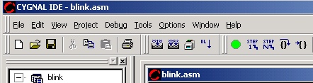
The Cgynal ide is working!
Csd is in the process of trying to the the Cygnal development
system working. After several hours of work last Saturday, csd gave
up.
On monday, however, a Cygnal apps engineer had csd reprogram the
flash on, not the target Cygnal 80C52, but the Cygnal 80C52 processor in
the serial adapter. Things are about working.
Track the
history of the Cygnal... and guess the time involved to get
this far. Not bad on this end.
The Cypress 3761development system illuminated a green LED on the
development board when the driver was apparently loaded on Windows 2000 start
up.
The green LED no longer appears but MEMTEST works. Hmm.
Tuesday February 5, 2002 14:16
Cormac
Glad to hear you guys are doing fine financially.
Neat product.
http://www.geocities.com/computersystemsdocumentation/
If I've made any mistakes, let me know and I will correct.
With the internal 4k ram a forth would work on the cygnal part.
Forth needs space for two stacks plus one heap. And four registers, W,
IP, RP, SP which are contained the registers.
The advantage to BASICs and Forth is that source code is compiled or assembled
by the target.
Looks like the Cygnal parts could do this REAL QUICK.
bill
Bill phoned Cormac.
Problem is that bill didn't hit the download button. When this
happened the green led blink app ran
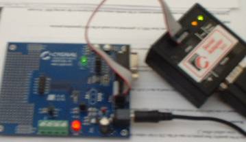
The red LED on the serial adapter turn to green, then the BIG LED
on the development board begins to blink.
Cormac elaborated on one of his emails
One thing I wanted to clarify from what I saw on your website about movx
instruction use on our website. You are right that we do not support execution
from external code memory.
As for the movx instruction, it provides access to on-chip FLASH memory,
on-chip external RAM, and off-chip external RAM through the External Memory
Interface. The External Memory Interface is currently only available on our
C8051F02X devices, you can read more about it in the
C8051F02X data
sheet available on our website.
C8051F020 25 64k flash has 4352 bytes of external on-board ram.
This is accessed by the -RD and-WR control signals.
In the system csd is testing only the 256 bytes of internal register ram
is available.
The size of the packaged Cygnal 80C52 is only about 1/8 inch square.
The sipex line driver chip is about 4x the size of the Cygnal chip.
One importance of taking this day or so digression is that on-board software
development as opposed to an emulator is a good way to go. The Cgynal
system is a cross development system in that code is assembled or compiled
on the PC, then downloaded to the Cygnal part.
What csd is aiming for is a system where source code is compiled and assembled
by the target.
So back to the Cypress development board.
Cygnal emailed csd its ECReset.zip which expanded into ECReset.exe.

Here's the serial adapater flash reprogrammer user interface.
Let's see if this works.
Cormac
Can we get the source code to ECReset?
This would save some time with possible future Cygnal ide projects.
Where?
bill
|
Embedded controller Forth for the 8051
family 1
will run on the Anchor/Cypress 3761 and 3861 development systems.
But how to get it working there?
Study of what Anchor/Cypress and Keil did is where we
start.
This project is starting to get
fun. Sunday February 3, 2002
09:30
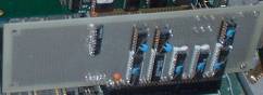
| Here' a commercial 8051 machine based on the schematics in Embedded
Controller Forth for the 8051 family.
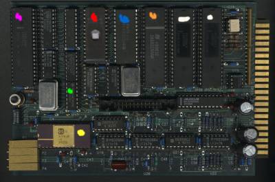
The chip with the pink dot is the 80C51. The green dot shows an
'HC00 which implements the Princeton architecture. The eprom
is dotted red. The 32kx8 RAM a blue dot. The National 82C50 UART
a orange dot. And two 83C55 ports white dots.
The yellow dot show location of a 754 A/D converter.
The machine reads digital signals, takes A/D conversion reading, then
outputs the information to a digital display and transfers information to
a PC over a serial port.
Improvements can usually be made to a design. The 754 is close
to the HC00 and unshielded.
It is better to digitize at the sensor where the converter has its own
regulated supply, convert to optical or opto-isolate rs-485, then
communicate back to the 8051.
The 8051 family is ideal for this because of its mode 0 serial expansion
bus. Many, if not most, A/D converter have serial data out.
These machines are working all over the whole. One even in
Hiroshima.
The operating system code is out of Embedded Controller Forth for
the 8051 which includes the romed assembler and even full screen
editor on the 8051.
The applications code is all in high-level forth. We didn't
have to go to assembler because the app ran fast enough in high
level. The app contains about 40 screens of forth.
Both the hardware and software are super-reliable. This system
have been running since about 1993. And made the customer, not
csd, lots of money!
There was practically no development time for both the hardware and
software. The hardware schematics and OS came out of the book.
In reality the speed of an operating system has little to do with how
fast an application works. Windows 2000 is a good example!
In most applications the operating system is the most-background task.
Idle time is spent in the OS. But when an interrupt occurs control
is immediately transferred to assembler language top-priority routine
for execution.
Task priorities are determined by the interrupt priority setting -
not software algorithms.
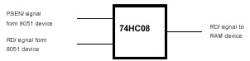
The Princeton or von Neumann architecture by ANDing of PSEN
and RD was done with a 'HC00 NAND gate rather than an 08. Why csd doesn't
remember. But a disadvantage is that the 00 has to be entered twice
to invert the NAND gate output thus increasing the gate propagating
time of PSEN# & RD#.
The Anchor/Cypress CY7C64313 does the ANDing on board
greatly decreasing propagation time!
The pdf help files in the Keil software contained
May 31, 2000, Munich,
Germany
by Keil Support, Keil Elektronik GmbH [email protected] ++49 89
456040-0
This Application Note describes the steps that are required to install
and use the Keil Monitor-51 on a user specific hardware.
The Keil Monitor-51 allows you to connect your 8051 hardware to the
µVision2 Debugger. You can use the powerful debugging interface to test
application programs in your target hardware.
For further information about using the Keil Monitor-51 together with
the µVision2 Debugger refer to the User’s Guide Getting Started
and Creating Applications with C51 (KEIL\C51\HLP\GS51.PDF), Chapter 11. Using
Monitor-51.
Hardware and Software Requirements
The following requirements must be met for Monitor-51 to operate
correctly:
8051 CPU or derivative
5 Kbyte external code memory (EPROM) starting at address 0 (loaded with
Monitor-51 software)
256 Byte external data memory (XDATA RAM) and 5 Kbytes trace buffer
(optional). Additionally, the external data memory must be big enough to
hold the complete application (code and data). All these external data memory
areas must be von Neumann wired, this means that access is possible from
XDATA and CODE space. A common way to do this is to connect the CPU signals
/PSEN and /RD to a AND gate. The output of this AND gate is then connected
to the /RD pin of the RAM.
Note that Keil calls the Princeton architecture the von Nuemann wired
1
2
3
4
See U4 in Sandia tech report.
4
Next csd finds in the Keil link and load documentation
The BL51 code banking linker/locator provides the following functions:
Combines several program modules into one module, automatically incorporating
modules from the library files
Combines relocatable partial segments of the same segment name into a
single segment
Allocates and manipulates the necessary memory for the segments with
which all relocatable and absolute segments are processed
Analyzes the program structure and manipulates the data memory using
overlay techniques
Resolves external and public symbols
Defines absolute addresses and computes the addresses of relocatable
segments
Produces an absolute object file that contains the entire program
Produces a listing file that contains information about the Link/Locate
procedure, the program symbols, and the cross reference of public and external
symbol names
The statement
Produces an absolute object file that contains the entire
program
implies that the linker builds a binary image of all of the compiled or
assembled program components.
Anchor/Cypress appear to have some type of an Intel Hex loader.
Csd finds a Keil ulitity OH51 which
Chapter 5. OH51 Object-Hex Converter
OH51 is an application that converts absolute object files into Intel
HEX files. Program code stored in the absolute object file is converted into
hexadecimal values and is output to a file in Intel HEX file format. The
Intel HEX file may then be used by an EPROM programmer or emulator.
The following sections describe how to use the OH51 program, the command-line
options that are available, and any errors that may be encountered during
execution.
Using OH51
To invoke OH51 from the DOS prompt, type OH51 along with the name of the
absolute object file. The OH51 command line must be entered in the following
format:
OH51 absolute_obj_file [HEXFILE (filename)]
where absolute_obj_file is the name of the absolute object file that is
generated by the L51 linker/locator.
filename is the name of the Intel HEX file to generate. By default,
the name given to the HEX file is the base name of the absolute_obj_file
followed by the .HEX extension.
The Nautilus 2 metacompiler puts out a binary image of the 8051 family
forth operating system. So the OH51 can be used to convert it.
Anchor/Cypress has two types of files which load on its development systems.
.hex and .bix.
Csd is still a bit unclear about the file formats and their orders so
csd did a bit of research on this.
Under Windows 2000 csd invoked the the 8086 family forth in Embedded
controller Forth for the 8051 family.
Csd located the binary image dump and listed it on the screen
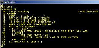
Csd then switched the primary image file to dev_io.hex and dumped the
first bytes
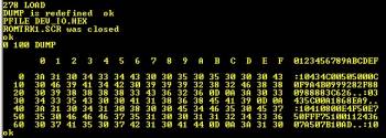
The switched to dev_io.bix and dumped
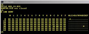
Looks like some of the interrupt vectors are getting patched in devio.bix.
The 4b long jump to 02400s appear to be a IC bus interrupt vector!
But as we see from the image that DUMP was either written or updated in
1986. DOS days.
We have to get the 8051 Forth first running under a Windows app for the
Anchor/Cypress development systems!
Then we have to upgrade the nucleus to a dual data pointer 80C52 forth!
A DOS window spawns a virtual x86 machine. Each DOS window opened spawns
a new virtual 86 machine.
Many of the utilities in the Keil development system are written as console
apps - you see a DOS-like window. You get to use printf in console apps.
Anchor/Cypress console app is written as a C windows application.
The Anchor/Cypress ezusbsys driver is written in C, not C++.
Compuware/Numega drivers are written as C++ program.
Csd writes its drivers in C++ and uses Compuware/Numega DriverStudio -
DriverWorks 2.0. Friday February 1, 2002
06:54 |
Musashi's advice
Develop intuitive judgment and understanding for everything
1
is applied to Cygnal's "black box" which goes between the development
board and PC.
Csd took it apart.
Inside is a voltage regulator. The Cypress 3761 also has on-board
voltage regulation (orange dot). This is a very good practical idea,
especially for powering circuits which contain a/d converters.
The original 8051 family is very noisy. PSEN again along with ALE,
AD7-0, A15-8, RD, WR. You can do a preliminary TEMPEST test with a
CB [10 meter radio] on your 8051 design.
Also inside is an ESD184E oscillator or crystal (green dot), a
Sipex
3223ECY 0050 5 volt rs-232 transceiver (blue dot), and, very interesting,
another Cygal C8051F012 T0AAOFDA0140 microcontroller (yellow
dot)! Friday February 1, 2002
06:33
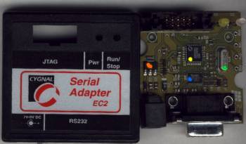
The top of the plastic case is to the right of the board.
The Pwr and Run/Stop LEDs are at the upper right.
The nine pin serial port connector is seen at the bottom of the board.
We hate to bring this up, but it is very important to shield a/d converters
from the 80C52 for noise reasons. One gets a rather large random number
component out of an unshielded a/d converter ... largely, we think, because
of PSEN.
So it will be interesting to test the Cgynal a/d converter to see how
it does since it is on the same die as the 8051. |
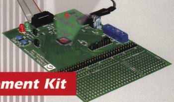
Csd's Cygnal Integrated products Development Kit
arrived early this morning.
Note!
Cygnal’s advanced pipelined 8051 CPU delivers the highest throughput
by executing most of its instructions in just one or two clock
cycles.
Csd has heard of 80C52s almost working that execute most
instructions in one of two clock cycles and run at 96MHz!!!
The memory model for Cygnal part uses PSEN. This is incompatible
with Embedded Controller Forth
1
which ANDs -PSEN and -RD. But this is what Anchor/Cypress did making
Anchor/Cypress 3761 and 3861 development kits capable of running this
Forth.
We at Sandia labs started
an internal Forth project [using PSEN] but never completed this. Hmm.
Zeitgeist?
Included with the Cygnal development kit is a plug-in wall power
supply adapter. Also the Cygnal uses a serial port.
The Anchor/Cypress 3761 and 3861 uses the power from the USB connector
and neat 3.3 volt design. This is really slick!
Csd speculates that ARM and other cores will not be very helpful
with the peripheral microcontroller is connected in a PC with USB 2.0
communications.
Reason is that computations can be made in the PC either at ring
3 in Visual Basic 6.0 or in ring 0 using C++ 6.0 and inline assembler using
super-fast USB 2.0 communication.
There is not much sense in lots of software in the peripheral controller.
This is too expensive and the development environments are much worse
than Visual Studio 6.0.
New PCs effectively are
-
Infinitely fast
-
Have an infinite amount of memory
-
Have an infinite amount of disk space
-
Cost practically nothing
-
Have exquisite Microsoft Visual Studio 6.0, Visual Basic, and C++.
Who wants to waste their time [and money] writing lots of
code on a peripheral microcontroller when one can do the work in
the PC?
But some code is required on the peripheral microcontroller. So
one wants a interactive operating system there. Forth is a prime
candidate.
Rules, of course, may change a bit for where lots of code resides
in peer-to-peer microcontroller application. But csd is into hooking
microcontrollers to PCs.
Csd is about ready to have lots of fun with both the
Anchor/Cypress system ... once Embedded Controller Forth communicating over
USB works, of course.
And the Cygnal mixed-signal communicating with the Anchor/Cypress
over mode 0[synchronous serial] or mode 1 [network] communications.
Words at the top of the Cygnal development kit box state
Capture
> Compute
>
Communicate
The integrated peripherals - timers, serial communications - sets
the 80C52 apart from other microcontrollers. And now high oscillator
speeds coupled with few clocks per instruction.
Wednesday January 30, 2002 09:34
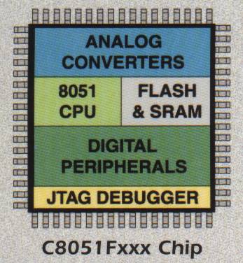
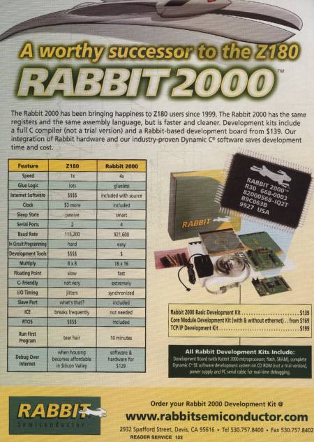
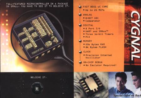
CYGNAL KITS
What designers want.
Cygnal kits contain everything you need to develop circuit applications
with Cygnal’s flexible C8051Fxx family of mixed-signal microcontrollers.
These exceptional devices integrate a high-speed 8051-compatible CPU with
in-system programmable FLASH memory and a rich complement of digital and
analog peripheral in a single package. Cygnal’s advanced pipelined 8051
CPU delivers the highest throughput by executing most of its instructions
in just one or two clock cycles. On-board FLASH memory can be used for both
program and non-volatile data storage (written at run time by user software).
Hardware digital peripherals include serial interfaces (SMBusTM /I2CTM, UART
SPI TM), timers, and programmable counter array. Analog peripherals include
A/D and D/A converters, comparators, voltage references and more.
EVERYTHING FOR YOUR
MIXED-SIGNAL. DESIGN
Cygnal's C8051Fxx products let you develop complex electronic systems
quickly and easily. The mixed-signal integration offered by our products
enables most of the user's system to be implemented in a single device. In-system
programmability also makes it easy to perform system software changes and
updates, either locally or remotely.
EXAMPLE APPLICATIONS
• Industrial control systems
• Medical instruments
• Process control equipment
• Communication systems
• Consumer products
• Automotive electronics
• Test and measurement equipment
• Computer systems and peripherals • Portable equipment •
Electronic toys
...and many, many more
All you need to run the Cygnal Development Kit software is a host PC.
System Requirements • Windows® 95/98/NT/Me
• 32Mb RAM
• 8Mb free hard drive space
• Free COM port
CYGNAL Integrated Products, Inc
Founded in March 1999, Cygnal Integrated Products, Inc. of Austin, Tx
designs, manufactures and markets advanced in-system programmable mixed-signal
System-on-Chip products and associated support tools.
These unique devices embody the company’s no-compromise attitude
and distinguished technical skill base integrating world-class analog high-speed
digital and FLASH memory functionality into a single powerful chip.
The combination of mixed-signal integration and in-system Programmability
offers tangible user benefits through higher component integration, greater
design flexibility faster time-to-market, superior system Performance and
improved end product differentiation.
Cygnal products deliver advanced application solutions expressly designed
to address a broad range of markets including communications systems industrial
equipment and consumer products.
Look! Practically NO PARTS!
 |
We read, think, study, and post. There is a reason for
this.
Develop intuitive judgment and understanding for everything
1
We think that Musashi suggests we have to do a bit of study and thinking
to understand what's really going on.
So let's hope these pages help us all really understand what's going
on with cores [80c52, arm, mips, novix, rtx2000, coldfire, 56k, ...], usb,
1394, 1284, serial ports, peer-to-peer communication, serial communications
... .
So those of us who understand can make some bucks and have a good
time making those bucks!
And may, of course, the
forth be
with
you!
Tuesday January 29, 2002 18:06
Csd is now studying Cypress's serial eeprom. The reason is
that csd want's to know as much a possible about the EZ-USB-FX boot
load
There is a lot of software on the cypress cd rom.
Included is the Anchor/cypress Monitor. This was written under
Visual C/C++ 5.0 but compiles just fine under 6.0 once the files are
converted.
The EZ-USB-FX has an
I2C
bus.
The I2C bus is connected to a serial eprom. Let's look at what cypress
did and eprom v ram considerations in general.
Monday January 28, 2002
19:59
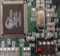
| Here's a photo of the socketed serial eeprom chip on the cypress
3761 development board.
We put a red dot on it to identify it from the CY7C64313.
Here's the schematic of the eeprom connect.
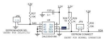
SCL is the I2C serial clock. SDA is the serial data. Both
of these signals come directly from the CY7C64313, pin 5 and 6
respectively.
JP 8 is open while JP 9 is shunted [jumpered].
Cds' 3761 board is populated by a a
Microchip
24LC00 serial eprom. As we can see from the datasheet,
the 24LC00 runs in the range of 2.5 to 6.0 volts. This is important
because the 3761 board runs at 3.3v.
The 24LC00 has the 8-pin PDIP/SOIC showing a NO CONNECT on pin 1 while
the 3761 has it jumperable. Hmm.
There are only 16 bytes available on the 24LC00. This is pretty
small.
Let's talk about the advantages and disadvantages of rom [prom, eeprom,
flash, etc] versus static ram.
At Sandia labs we populated
the motherboard with 32kx8 bytes
of static ram and 32kx8 bytes of eeprom. But we also shadowed the eeprom
with a second 32kx8 eeprom on the
maintenance support board.
We did a romed system. The 8051 forth operating system was mostly
contained in rom. Code executed out of the rom.
We were able to load eeprom programming software into ram, then have the
forth operating system program itself on to the eeprom on the motherboard.
Romed operating systems are a bit more complicated than ram-based operating
system.
At the time we did our early forth work, about 32kx8 roms and rams were
about the largest capacity available.
We need to minimize chip count so we put the code in rom.
However, when 64kx8 rams became available, then we could have the same
chip count and copy the eprom into ram shortly after coming out of reset.
One advantage of rom is that you can't easily write into it. So
the rom software may be a bit more safe from accidental over-writes. On
the other hand, the rom software is difficult to change.
Cypress is about a ram-only system. All 128kx8 bytes of it! The
CY7C64313 can only handle 65kx8 of it.
Is a romed system more reliable in the field than an all ram system?
We'll see.
We will cover how the 3761 handles its bank select [BANK0 out of the 22V10]
as we proceed.
So the 3761 apparently has the ability to both read and write to the serial
eeprom.
There is a lot of code to be understood in the 3761 development system.
This takes time. Much if not most of the code on the cd rom
is source code.
But understanding how the 3761 work may require a bit of research
too. Dumps and disassembly.
Keil software has a neat MEMTEST c example. Lots of LEDs blink and
"good" is spelled on the 7-segment display if the test is successful.
However, if you try to build the binary the Keil software will not produce
the output hex file. The reason apparently is that it exceed s 4 k
bytes in size.
Keil only supplies a trial version of its c compiler.
This unfortunate great software cost is not lost on other hardware/software
vendors!
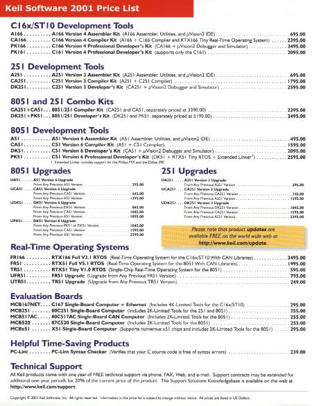
which makes a big deal of "trial version" compilers. See the $$$
v $ in Development Tools in the table.
We've got to try to
reduce
the cost of an operating system, compiler, and assembler for the
Anchor/Cypress 3761 and 3861development boards! |
Custom analog chip designers may need an on-board microcontroller
to handle "hardware-herding" duties.
Two the the main microcontroller cores are the
ARM
and 8051 cores.
The 8051, 80C52 really, is nearly a public-domain core. This
makes it very attractive. Especially since there is source code interactive
real-time operating system written largely in a high-level language, incremental
compiler and assembler, loader and linker available.
1 Monday January 28, 2002 20:03
Cygnal Integrated Products, Inc
4301 Westbank Dr., Suite B-100
Austin, Texas 78746 USA
Tel. (512) 327-7088
Toll free (877) 9CYGNAL
Fax (512) 327-7087
www.cygnal.com
Cygnal includes a die in the transparent window. It is about 1/8 inch
on each side.
The 8051 family is well-suited to high G applications like Sandia lab's
earth penetrator. 68K family processors dies break in high G tests.
Note that Cygnal, too, touts "No emulator required."
Modern users will demand to be able to "log on" to their peripherals into
interactively interrogate them to find out what may be going wrong.
Engineers simply cannot anticipate all of the failure modes. Binary
diagnostics included in microcontroller app code is not the way
to go.
The way to go is interactive access to the hardware perhaps coupled
with source code compilation of diagnostics on the peripheral microcontroller.
You may be looking for port pins which should, but don't toggle, strange
stuff in buffers, messed-up state tables, things that you just can't predict
in advance. We have experienced in this!
4 Been there, done
that! |
Csd has the problem on ANDing PSEN# and RD#, not
Cypress.
Csd received the cd rom by FedEx today from Cypress!
Csd made a back-up of the old cypress directory, then installed the
software.
The software is huge in comparison to the previous
download.
Csd then checked the new schematics with the old. They appear
to be the same.
Look at pin 6 on the PAL which is PC6. That's RD#.
While Cypress routed OE# into the PAL, RD# is also routed into the
PAL.
Csd's misconception corrected.
So we're on to the next interesting thing.
CLKOUTR going into pin 2 of the PAL.
Wednesday January 9, 2002
20:47
Here's the CLKOUT description
34 19 12 CLKOUT O/Z 24 MHz Clock Output
This is the 24- or 48-MHz clock, the master clock for the 8051, phase
locked to the 12-MHz XIN/XOUT clock.
(Note: the GPIF always uses a 48 MHz clock or XCLK, regardless of the
8051 clock. See XCLK and XCLKSEL.)
The frequency of the 8051 clock is set via a boot EEPROM bit:
If Config 0.2 = 0, CLKOUT is 24 MHz.
If Config 0.2 = 1, CLKOUT is 48 MHz. CLKOUT may be inverted by setting
a boot EEPROM bit CONFIG0.1=1.
If no EEPROM is connected to the I 2 C compatible port (the required
pull-up resistors must be present), the Config0 bits default to zero, hence
- CLKOUT is 24-MHz
- CLKOUT is non-inverted.
The 8051 may three-state this output by setting CPUCS.1=1.
Here's the relevant portion of the schematic
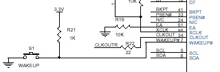
Note the apparent 22 ohm current limiting resistor at CLOCKOUT pin 34.
Also notice that EA is pulled to ground through a 10k resistor.
Note in the old 8051 design EA
was strapped to either Vcc or ground. Hmm, who's right?
Here's the EA description.
51 EA Input N/A External Access This pin determines from which memory
the 8051 fetches CODE when a CODE fetch is in the lower 8051 address space
(CODE addresses 0x0000 to 0x1B3F):
If EA=0 the 8051 fetches CODE from internal RAM.
If EA=1 the 8051 fetches CODE from external memory (normally used to
boot from external memory, for example, boot from Flash).
See PSEN# pin.
(EA is tied to GND internally in both the 80- and 52-pin packages.)
Here's the PSEN# description.
33 PSEN# Output H Program Store Enable PSEN# strobes LOW when the 8051
fetches a CODE byte from external memory.
If EA=0, the 8051 fetches CODE from external memory from 0x1B40 to
0xFFFF.
If EA=1, the 8051 fetches CODE from external memory from 0x0000 to
0xFFFF.
See EA pin
CLKOUTR goes into
pin 2 through R10.
Notice that there is a voltage divider between R10 [whatever N1 is] and
R12 [10k]. Why?
Why R22 and R10?
And why is CLKOUTR going into pin 2 of a
22V10?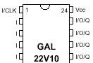
It looks like a clock may go into pin 1. This from Lattice's data
sheet on the 22V10.
Why is the voltage divider necessary?
Here's a schematic of the 22V10
Why isn't CLKOUTR going into pin 1 rather than pin 2?
The currently beats us. For now.
Glenn! Do you know answers?
And thanks guys so much for the cr rom by fedex!
The new cd rom contains tons more code examples than the
download.
Cypress is now using Compuware/Numega DriverWorks!!!
This is what csd uses.
These wdm - peripheral projects are getting so complicated that one can
not expect to, or even try to, do them alone. |
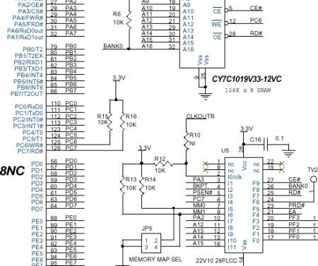
The reason cypress put the chip decoding in a pld is that some, probably
very few, if any, might want to change to use other memory models.
Cypress has the right idea, we believe. Convert a "Harvard"
architecture into a "Princeton" architecture.
Note also the banked 128k x 8 sram! No need for the original
64 x 8 code and 64 x 8 sram.
Let's continue try to get a specific answer out of cypress.
Cypress, of course, is concerned about product recall.
Intel lost big bucks with the numerical co-processor problem several years
ago
Glenn is a manager.
Friday January 4, 2002 17:47
Hardware bugs are usually lots more expensive to fix than
software bugs.
Now that we have internet and microcontrollers like the Cypress CY7C64613
the cost of fixing microcontroller software bugs should decrease.
The development board works just fine. But let's see what Cypress
says. Thursday January 3, 2002
10:11
Friday 1/4/02 3:56 PM
Glenn
I respond to
The FRD signal has nothing to do with a standard 8051 memory interface,
I do not know why you mention it.
Your statement is valid.
I had to go to the cypress product CD rom to find the right RD#. It's
pin 126. Here's the description from the cd rom
126 76 51 PC7 or RD# or CTL5 I/O/Z I (PC7)
Multiplexed pin. Function selected by bits: PORTCCFG.7, PORTCCF2.7 and
IFCONFIG[1..0]. PC7 is a bidirectional I/O port pin. RD# is the active-LOW
read strobe output for external memory. CTL5 is a GPIF output signal.
If RD# is chosen as the function of this pin, it should be pulled up to
V CC through a pull-up resistor. This is to ensure that RD# is in-active
(pulled HIGH) at power-up, since, before the 8051 can con-figure this pin
to RD#, it defaults to 'PC6 an input'. 128 80 52 Name Type Default
Description
I see the 10K R16 recommended pull-up on the schematic below.
Now that we have this cleared-up, I continue to believe that pin 126,
RD#, should be connected to pin 3, in stead of PA3, OE#, to correct the
circuit.
The reason I spend time to view the cypress schematics is that I want
to be reasonably sure that I understand the decoding before trying to port
an 80C52 forth operating system to the board.
The metacompiler '51 source must be adjusted to avoid memory used by the
CY7C64613.
While I'm sure your statement
We have sold thousands of FX Dev Kits without our customers ever encountering
the issues you raise. Further, we have sold Millions of FX parts, without
a single return due to design issues, or part failure.
is correct, I feel that we all still need to have a specific explanation
why OE# connection is correct and RD# is not.
I await Cypress's reponse.
Thanks
bill
Thursday 1/3/02 9:26 AM
Glenn
I may have found a problem in the CY3671 EZ-USB-FX development board
schematics.
I would like to get Cypress's comments on this.
Reason is that if my concerns a valid, then there is a partially-benign
bug in the CY3671.
The problem involves ANDing -psen and -rd to overlap code and data
memory.
I write "partially-benign" because the ANDed -psen and -rd may be
unnecessarily ANDed again in the 22V10 PLD.
Let's look at the schematic
Look at PA2 which goes into pin10 of the 22V10.
Look at PA2/#OE which comes out of pin 27 on the CY7C64613.
Look at CE# which comes out of the 22V10 on pin 27. CE#
apparently goes into pin 5, -CE, on the Cypress CY7C1019V33 128k x 8 sram.
Now let's look at some PAL equations.
modesw = [mm1,mm0]; " two dipswitches indicated memory map
equations
!nPRD = !nDRD # !nPSEN; " combined code/data read strobe
BANK0 = 1; " unused, drive high to saves power
WHEN (modesw == 00) THEN " No external memory
{
nCE = 1;
nRD = 1;
EA = 0;
}
ELSE WHEN (modesw == 01) THEN " Ext P&D mem at 8000 (can add mem to
0-8K)
{
!nCE = A15; " selects upper 8KB
!nRD = !nDRD # !nPSEN; " Combine program & data memory
EA = 0;
}
ELSE WHEN (modesw == 11) THEN " Ext P&D mem at 0000 and 8000
{
!nCE = 1;
!nRD = !nDRD # !nPSEN;
EA = 0;
}
ELSE WHEN (modesw == 10) THEN " All program mem external
{
!nCE = 1;
!nRD = !nDRD # !nPSEN;
EA = 1;
}
test_vectors
([nDRD,nPSEN] -> [nPRD])
[ 0 , 0 ] -> [ 0 ];
[ 0 , 1 ] -> [ 0 ];
[ 1 , 0 ] -> [ 0 ];
[ 1 , 1 ] -> [ 1 ];
The equations and test vectors are fine but it appears that PA5/FRD,
PA5 coming out of pin 30 of the CY7C64613 is not going into the PAL.
Rather PA2/#OE which comes out of pin 27 goes into the PAL.
Cypress documentation states
• OE# goes low when RD# or PSEN# goes low.
This appears to suggest to me that PSEN# is unnecessarily being ANDed
with RD#.
What I think should happen is that PA2/#OE which comes out of pin 27 should
go directly to into pin 5, -CE, on the Cypress CY7C1019V33 128k x 8 sram.
Please let me know Cypress's comments.
I'll post this on internet so it will be easy for others to view and
comment.
best and onward
bill |
Bob Dixon of Addem's
package containing Cypress UBS 2.0 Solutions, Making USB Universal; Making
USB Universal booklets, and a cd rom titled Making USB Universal arrived
this afternoon.
Csd bought its EZ-USB-FX2 from Future electronics. The part
number is of the FX, not FX2, is CY3671.
The FX 2 part number is CY3781. This is the board to
order. Tuesday January 8, 2002
19:16
[email protected]
http://www.addem-az.com
The FX2 development system looks very similar to the FX board. But
there are differences.
You want to order the CY3681.
Here's the technical differences between the FX and FX2 taken from the
cd rom slide show Monday January 7, 2002
14:15
 |
Csd discovered that the CY3671 EZ-USB-FX development board schematic
it has does not match what's on the board.
It is fairly important to understand the hardware before writing
software.
Here's an interesting case of not taking, or be able to take, the
time to analyze what's really going on.
1
Monday January 7, 2002 06:36
Adios ALE!
ALE
Address Latch Enable output pulse for latching the low byte of the address
during accesses to external memory.
In normal operation ALS is emitted at a constant rate of 1/6 the oscillator
frequency, and may be used for external timing or clocking purposes. Note,
however, that one ALE pulse is skipped during each access to external Data
Memory.
The Cypress CY7C64613 doesn't have an ALE since the address lines A7-A0
aren't multiplexed with the data!
But this brings us back to PSEN, memory speed, external decode and brings
up the subject of product recall.
Monday January 7, 2002
06:20
The old 8051 ran at 12 MHz.
This is roughly 83.33 nanoseconds per clock.
The old 8051 took 12 clocks to complete most instructions. So that's
1 microsecond for each instruction.
But as we know PSEN is output twice! This means that the memory
must respond in less than 500 nanoseconds.
This speed was even pushing some of the old eproms.
The CY7C64313 is running at 48 MHz [or maybe 24].
At 48 MHz is 20.83 nanoseconds.
The CY7C6431 only takes 4 cycles to complete most instructions. 4
* 20.83 = 83.33 nanoseconds.
However, PSEN is coming out twice so the memory must respond within
less than 41.66 nanoseconds.
Here's the
memory
datasheet. 12 nanoseconds looks to the response time.
Memory read response depends on when chip select [-CS] and [-RD ... the
memory read, not the 8051 -PSEN & -RD] so its super-important
to get these signals to the memory as soon as possible!
This is why CY7C64313 develops both PSEN# & RD# and CS# on-board.
But the development board forms both on a
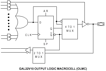
PAL.
More on the
22V10
used on the development board.
Cypress and csd are discussing a possible bug on the CY3671 EZ-USB-FX
development board. This possible bug involves off-chip memory read
strobe and chip select.
Csd also discovered that when Vendor
Request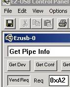 is clicked, EZ USB control panel
locks-up so badly that windows 2000 can only be fixed by a hard reset. is clicked, EZ USB control panel
locks-up so badly that windows 2000 can only be fixed by a hard reset.
Later csd left control panel in its apparent locked-up condition. It
recoverd in about a half hour.
This problem is much less expensive to fix than the possible PAL input
signal problem.
This leads us to product recall. Ford Explorers and Firestone
are both fresh in our minds.
Here's another unfortunate recall notification that reached bill
yesterday
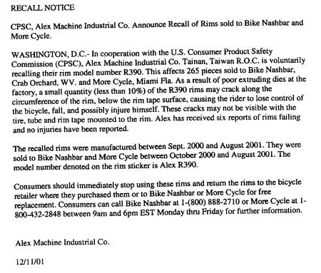
Ouch! Look at Alex's potential problem
1
2
... We smell
lawyers.
Hardware screw-ups are very expensive to fix. Software screw-ups
less expensive.
Besides you don't call them 'bug fixes.' You call them "service
packs."
Advantage of doing things in software compared to hardware for complicated
things, like USB protocol, is that unfortunate errors are easier and less
expensive to fix.
We, of course, must watch
Cypress
stock carefully as a potential product recall develops.
T J Rogers made a neat
decision to buy Anchor. We continue to believe. Pending
finding other problems, course. |
Perils of PSEN.
PSEN#
Program Store Enable is the read strobe to external Program Memory.
When the device is executing code from external Program Memory, PSEN is
activated twice each machine cycle, except that two PSEN activations are
skipped during each access to external Data Memory. PSEN# is not activated
during fetches from internal program memory.
Intel 8-bit Embedded Controllers 1991
The Cypress CY7C64613 is the motherboard seen at
1 put on to a single chip with USB
and other peripherals. So let's look at the importance of PSEN.
Saturday January 5, 2002
09:26
The original 8051 family oscillator was 12 MHz.
An instruction cycle consumed 12 clocks.
Suppose the instruction ANL A, # 12 [A # 12 ANL in Forth assembler]
is located at addresses 1000 and 1001
ANL is represented hex 54 so in memory
1000 54
1001 12
When the instruction counter is at 1000 the address is asserted on the
high 8 bit address lines A15 - A8 and the 8 bits on AD7-AD0.
The ALE [address latch enable] goes low latching the address in the external
latch seen at chip U1. Now
that the address is set up, the 8051 must read the 54.
PSEN# goes low TLLPL = 43 nanoseconds, more or less, after ALE goes low.
The 54 is read into the 8051 about TPLPH = 205 nanoseconds later.
Keep in mind that the ANL immediate is executing in one instruction cycle
or about 1 microsecond. So at the point that the 54 is in the 8051
about 500 nanoseconds have elapsed.
The program counter is incremented to 1001. And the same processes
is repeated to read the 12 into the 8051.
The important message is that PSEN# is being activated about every
500 nanoseconds.
PSEN is strobing lots faster than RD#.
If the program is in external memory as it is the overlapped memory model,
the PSEN# must be ANDed with RD#. It takes time to get through an HC
'08 AND gate.
Memory must respond within the time the address is latched, chip select
asserted along and PSEN# AND RD#.
The problem to be solved is getting chip select and PSEN# AND RD# all
asserted in time to fast enough sram.
Old 8051 parts had 40 pins PSEN# and RD# were two of the output pins.
So PSEN# AND RD# had to be done external to the chip.
Most of the faster new 80C52 processors retained the 40 pin format.
Faster parts ran 24 or more MHz.
csd experimented by plugging-in increasing fast crystal oscillators into
overlapped code and external data 8051 machines running forth.
Forth stopped working at the higher oscillator frequencies.
Reason is that control signals were not reaching the memories in time
and/or the memories were not responding fast enough.
What could be done? Very little.
Faster logic like ALS might help. But this was not a good solution.
So csd did nothing. Execpt wait.
But now look what happened in the cypress CY7C64613.
All of the required external signals, PSEN# AND RD# and chip select
are not internal to the chip. The wait is over.
External memory Forth can now run again on the super-fast [48Mhz, 4
clocks/cycle] cypress 80C52 microcontroller! And hopefully will soon.
Reasons for this project include
1 80C52 Forth is an interactive real-time operating system.
2 Code take about 1/10 the memory as assembler or C code.
3 Code development is about 10x as fast as with a cross-development
environment.
4 Development system cost will be nearly free.
csd will post the 80C52 Forth metacompiler target source on internet.
5 The 80C52 Forth can compile, assembler, load and link source code.
Updates to the microcontroller operating system and/or application can
now be in source. This is opposed to a binary download.
6 Forth operating systems are very reliable.
7 csd likes to make money for both it and its customers by getting code
at the 80C52 microcontroller side, PC wdm driver, dll, and Visual Basic 6.0
side done quickly and painlessly.
8 It's more fun to do projects with little work opposed trashing one's
self using inappropriate software technology. |
The CY3671 EZ-USB-FX development system include a hardware breadboard
[both sides] pictured below.
The 80C52's are super i/o processors. In fact, the primary
role of the 80C52 is acting as a traffic cop for scheduling i/o operations.
Especially powerful old features was the synchronous serial mode
0 expansion bus.
On the old 12MHz 8051 parts the serial bus ran at a 1 Mbit rate.
The new fast parts many times faster.
Here's an example of mode 0 synchronous 8051 communications used
to load the read contents of shift registers
1 included in a Sandia Labs
tech report 2.
csd is looking to put serial-out a/d converters on this board for
digital sensors used in electrically-noisy environments.
Communications medium will likely be fiber optic. Wires don't
work very well in electrically-noisy environments. Noise can propagate
into the digital electronics at the microcontroller .
Friday January 4, 2002 09:29
Here's more details about how Cypress demultiplexes the 8052 address
bus, ANDs psen# and rd# on-board, and generates a chip select
on-board.
The cypress cd rom has a bug. You get directed to subject area.
Then to a specific part. Not the one you wanted to see.
To correct this, get into Windows explorer, look at the cd directory,
then click on the usb info.
We, of course, live in the real world.
Wednesday January 2, 2002 19:06
| The Cypress cd rom has detailed descriptions of the CY7C64613.
—Expanded interrupt system
—Two data pointers
• 3.3-volt operation
• Smart Serial Interface Engine (SIE)
—Handles much of the low-level USB protocol in logic, simplifying 8051
code
• General Programmable InterFace (GPIF)
—Allows direct connection to most parallel interfaces: 8- and 16-bit
wide
—Eliminates external glue logic in most applications
—Programmable Waveform Instructions and Configuration Registers to define
waveforms
—Six Ready (RDY) inputs and six Control (CTL) outputs
• Expanded Vectored interrupt system expanded for USB, FIFO flags and
DMA interrupts
• Separate buffers for SETUP and DATA portions of a CONTROL transfer
• Integrated I 2 C compatible controller
—400-kHz or 100-kHz operation
• Enhanced I/O
—I/O port registers mapped to 8051 SFRs (Special Function Registers)
for high speed bit operations
—Port bits can be controlled using 8051 bit addressing instructions
—Up to five 8-bit I/O ports
• Four integrated 8-bit-wide FIFOs
—Each 64 bytes deep
—Automatic conversion to and from 16-bit buses
—Easy, glueless interface to ASIC, DSP ICs and external logic
—Brings glue FIFOs inside for lower system cost
—Internal or external clock
—Synchronous (using strobes and a clock) or asynchronous (using strobes
only)
• DMA Controller
—Moves data between slave FIFOs, memory, and ports
—Very fast transfers—one clock (20.8 ns = 48 MHz) per byte for
internal transfers
—Can use external RAM as additional FIFO (accessed via Address and Data
buses)
• Special Autovectors for DMA and FIFO interrupts
• Glueless external memory expansion
—Up to 16-bit address bus and 8-bit data bus (see Table 1-1)
—Strobes RD#, WR#, OE#, CS# and PSEN#
—Buses not multiplexed (as in standard 8051), saving one clock per external
memory cycle
• Three package options—128-pin PQFP, 80-pin PQFP, and 52-pin
PQFP
Of extreme interest is the demultiplexed address bus.
Address lines A0 through A15 come-out of the 128 pin part.
The is a vast improvement of having to use an external transparent latch
to latch the low 8 address bits when -ALE goes low. You can see an
example of the latch chip U1, the
'373.
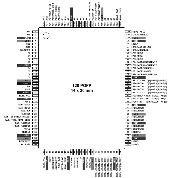
pin 126 pc7/rd#, 125 pc6/wr#, pin 33 psen# are standard 8051 family
pins.
rd# and psen# need to be ANDed to overlap code and data memory. This
is seen in chip U4, pins 9 and 10.
Another advantage of the CY7C64613 is that pin 27 oe#
• OE# goes low when RD# or PSEN# goes low.
means that the AND is internal to the chip.
And if only a single sram is used
• CS# goes low when RD#, WR#, or PSEN# goes low.
pin 28 cs# eliminates the need for external chip decoding. See chip
U9 which was required to
distinguish between EPROM, RAM, and memory-mapped I/O space.
So the old 8051 motherboard has
been eclipsed by a single chip. The old 8051 motherboard brought-out
all 8051 port signals to an XT bus.
The Cypress CY3671 EZ-USB-FX Development board Rev D bring the port signals
out ATAPI/EIDE, parallel port, serial ports, I^2C, USB, and other headers.
To show what an improvement this is, here's a discrete implementation
of an ieee 1284 port for the old 8051 motherboard.
So the Cypress CY3671 EZ-USB-FX Development board Rev D is a vast improvement
over the old 8051 system. |
Anchor/Cypress apparently developed the EZ-USB-FX chip, development
board, USB 8052 boot software, a windows driver, and demonstrations application.
Then sought outside help for system software. Here's a
summary. Wednesday January 2,
2002 09:50
The Anchor monitor software should or must be installed before
 plugging in the Cypress
CY3671 EZ-USB-FX Development board Rev D. plugging in the Cypress
CY3671 EZ-USB-FX Development board Rev D.
After the monitor is installed and you start windows 2000 from a PC power-on
condition you see windows loading, then you see a green LED light on the
Development board
This apparently indicates that Windows plug and play has done its enumeration,
found the development board, then loaded the Anchor monitor into the development
board.
Now you can run the Anchor USB test software
The Anchor development board exercise app is pictured at the left. In
front is the help. Help brings-up Microsoft Internet explorer so that
you can view Anchor/Cypress hltm help.
The help documents was produced with Dreamweaver 3.
Apparently at this point Anchor/Cypress sought help for software development.
Keil software was chosen with its C development platform,
µVision2.
Keil has an RTX-51 Real-Time Operating Systems. But that's going
to cost you some several thousands of dollars to obtain.
And, almost certainly, Kiel will not give you the source code to its operating
system.
Forth source, of course, for an 8051 family operating system is available
in
a
book available at Walmart!
The source code for the operating system and metacompiler which metacompiles
it has been reported posted on BBSs in the US, Sweden, Holland, and
Portugal.
C is known for consuming lots of memory for getting little done.
The same is true of assembler.
Forth, on the other hand, is the most memory efficient operating systems.
Memory efficiency is very important when overlapping code and data memory
in an 8051 system as Cypress/Anchor did with its CY7C64613. |
The Cypress CY3671 EZ-USB-FX Development board Rev D is the motherboard
seen at 1 is put on a single chip,
the CY7C64613 and upgraded with the newest 8052 peripheral technology. USB,
ATAPI/EIDE, I^2C.
csd has archived many of its main page articles.
We will focus is on the CY3671 EZ-USB-FX Development board Rev D,
wdm drivers, C++ wdm driver/Visual Basic interface dll, and Visual Basic
apps because of its great importance to peripheral-side hardware interface
to wdm drivers.
We'll also continue to post other relevant articles too.
Tuesday January 1, 2002
21:08
Inventing new microcontrollers usually is not a good idea from a
money-making standpoint.
SMC's main competition in the floppy disk controller/2 serial port/
parallel port chip business is Winbond.
csd contacted Winbond for a manual on their i/o chip. Winbond
responded that they didn't have one. They recommended we get the manual from
SMC. Clearly a clever way to save money.
Winbond builds an 80C51 which csd has used.
The problem all of these 80C51/2 vendors must solve is now the software
problem.
Having an operating system on an 80C51/2 speeds product to market
and maintainability by about an order of magnitude.
Once you've worked with an interactive operating system such as BASIC52
or forth, then returning to a development system is not a pleasant thought.
Or realistic in our internet world.
One wants to be able to log on to a problem 80C51/52 controller over
internet, then interactively debug a hardware or software problem.
If a software problem is encountered in either the 80C51/2 code or
Windows wdm driver, then repaired or improved version is posted on
internet. Tuesday February 13, 2001
09:36
Highly Integrated ARCNET Microcontroller And Network Interface
With 8051 Architecture For Embedded Applications
The COM20051I is a low-cost, highly integrated microcontroller with a
high-performance net-work controller based on the ARC-NET Token Bus Standard
(ANSI 878.1). Based on the popular Intel 8051 architecture, the device is
ideal for distributed control networking applications found in industrial
machine controls, building/factory automation, consumer products instrumentation
and automobiles. The COM20051I adds a fully-featured, robust, powerful and
simple network interface with basic 8051 peripherals including serial ports
and counter/ timers. The COM20051I also has an extended operating temperature
range.
Standard Microsystems Corp. (SMSC)
80 Arkay Drive, P.O. Box 18047,
Hauppauge, NY 11788-8847 USA,
Phone: 1-800 443-SEMI
ECN FEB 2001 www.ecnmag.com < This web address bombs IE5.0. The
real world again. |
The 8051 family is a "Harvard" architecture microcontroller.
There is separate code and data memory.
Program fetches strobed with PSEN-bar[bar over top of PSEN[program
store enable], Intel notation, bring instructions from the code memory into
the 8051 family microcontroller. PSEN-bar is also denotes -PSEN or
PSEN# to show that the signal is an active low.
PSEN is activated twice each machine cycle. Thus a two byte
instructions can execute in one machine cycle.
An example is ANL A, # 3 or in Forth pc/assembler A # 3 ANL which is
hex 5403.
Data read and writes are controlled by -RD aka, RD#, OE# or -OE and
-WR.
Since Cypress's goal is to download microcontroller over a usb connection
from a PC, it is important that code can be written and read from
sram.
Cypress EZ-USB-FX Family Development Board CY3671 overlaps code and
data memory.
This a modern-day version of overlapped code and data memory model
described in Embedded Controller Forth
1!
See pins 9 [-PSEN] and 10[-RD] of U4 in an 8051 family application
1 included the the Sandia tech report
1.
csd's experiments with fast [about 30-40 MHz] Dallas and Winbond
80C52s revealed that the propagation delay though a cmos HC'08 was to great
for reliable operation.
csd was faced with redesign of hardware or wait until someone else
designed new boards using the overlapped code and memory space idea.
Cypress engineers did the hardware engineering and board development
for csd!
Cypress used a 3.3 volt 22v10 PLD to AND -psen and -RD. This
apparently makes the output fast enough for Cypress's 48 MHz clock at 4 clocks
per cycle part compared to the orginal 8051 consuming 12 clocks at about
12 MHz.
csd and others have buy-out boards for applications!
Designing and building your own boards should be avoided if
possible.
And csd learned that Cypress put a General Purpose
Interface engine on their chip which the development board
interfaces to an 1284 parallel port connector and ATAPI/EIDE
header! Monday December
31, 2001 17:05
Let's look at what Cypress wrote about psen and rd and make some
clarification or maybe even some correction.
3.2 8051 Memory
Figure 3-1 illustrates the two internal EZ-USB FX RAM regions. 6,976
bytes of general-purpose RAM occupy addresses 0x0000-0xlB3F This RAM is loadable
by the USB core or 120-compatible bus EEPROM, and contains 8051 code and
data. The EZ-USB FX EA (External Access) pin controls the placement of the
bottom segment of code (PSEN) memory — inside (EA=0) or outside (EA=1)
the EZ-USB FX chip. If the EA pin is tied low, the USB core internally ORs
the two 8051 read signals PSEN and RD for this region, so that code and data
share the 0x0000-0x1B3F memory space. If EA=1, all code (PSEN) memory is
external.
3.2.1 About 8051 Memory Spaces
The 8051 partitions its memory spaces into code memory and data memory.
The 8051 reads code memory using the signal PSEN# (Program Store Enable),
reads data memory using the signal RD# (Data Read), and writes data memory
using the signal WR# (Data Write). The 8051 MOVX (move external) instruction
generates RD# or WR# strobes.
The statement "If the EA pin is tied low, the USB core internally ORs
the two 8051 read signals PSEN and RD for this region" is correct because
PSEN and RD are negated at the output pins of the microcontroller. deMorgan's
law states not[a or b] = not a and not b.
The manual goes on to explain
The USB core gates the standard 8051 RD# and WR# signals to exclude selection
of external memory that exists internal to the EZ-USB FX part. The PSEN#
signal is also available on a pin for connection to external code memory.
Some 8051 systems implement external memory that is used as both data
and program memory. These systems must logically OR the PSEN# and RD# signals
to qualify the chip enable and output enable signals of the external memory.
To save this logic, the USB core provides two additional control signals,
CS# and OE#. The equations for these signals are as follows:
• CS# goes low when RD#, WR#, or PSEN# goes low.
• OE# goes low when RD# or PSEN# goes low.
Because the RD#, WR#, and PSEN# signals are already qualified by the addresses
allocated to external memory, these strobes are active only when external
memory is accessed.
The statement "These systems must logically OR the PSEN# and RD# signals
to qualify the chip enable and output enable signals of the external memory."
appears to be in error. "AND" should be substituted for "OR."
But we live in the real world where the schematics sometimes don't match
what's on the board! Or mistakes are made in documentation. We
all make mistakes!
But the real importance is that the code from Embedded Controller FORTH
for the 8051 family can be made to run on the EZ-USB-FX Family Development
Board CY3671.
Operating systems for computers are generally developed one of two ways.
The first approach [Windows 9x series, Bill Gates' BASICs, BASIC52,
...] is a brute force building of an operating system binary from the linked
output of high-level and assembler code.
The second approach [Windows NT, 2000, XP Mach kernel] is to write an
operating system compiler, aka a metacompiler, which compiles both assembler
subroutines and high-level code definitions to an operating system binary.
Embedded controller Forth covers the later compiler method showing how
the Nautilus 2 metacompiler works.
Unlike many other real-time operating systems, Forth incorporates an
incremental high-level language compiler and assembler along with a loader
and linker.
C++ has similar features to Forth with its constructors and destructors
which allow dynamic code loads and discard which will be super-useful with
Cypress's USB communication capabilities.
And, of course, there is an about order of magnitude less cost of Forth
code development compared to the more traditional methods. Also, experience
has shown that Forth software is about an order of magnitude more reliable
than code produced with more traditional technologies. |
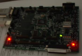
csd downloaded code for the
Cypress
EZ-USB-FX Family Development Board CY3671 REV D, S/N 1812C.
Within several hours a windows 2000 PC was communicating with the
Cypress board over USB.
A FujiFilm
FinePix 2300
was connected to a second USB port. This was used for the below photo
of the board.
Development of hardware and software on the target machine is perhaps
the best method.
Programs can run on a emulator and not on the target
machine.
When software or hardware stops working on a target, then one can
use an interactive operating system to find problems.
Tuesday December 25, 2001
12:30
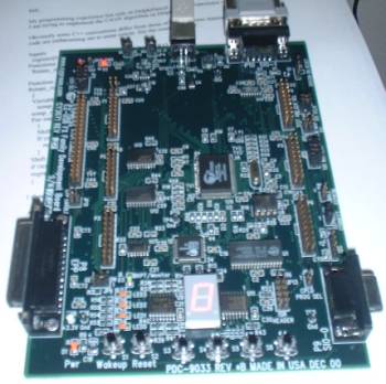
The USB connector supplies power to the board.
Serial port COM2 must be connected to the PC COM2.
At the right of the board in front is COM1 port. At the left is
a parallel port connector.
The Cypress html documentation was viewed with IE 5.5 while interactively
configuring the board. Csd first ran Cypress's board test. This requires
only the USB connection.
|
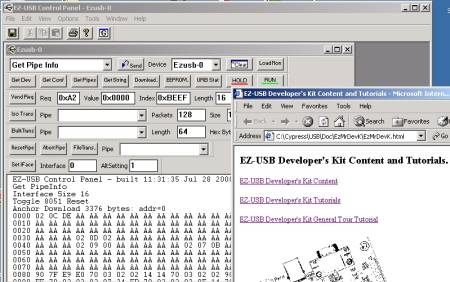
The Keil software is moved to a separate table.
Reason is that when the
Cypress
EZ-USB-FX Family Development Board CY3671 REV D first comes-up, it uses
the Anchor boot code to load additional code.
In the below example Keil software is loaded. But another operating
system, such as an 8051 Forth operating system could be loaded.
Wednesday January 2, 2002
08:30
The Csd ran Keil software demonstration program. This requires com2
connection. Here's a jpg of the Keil environment.
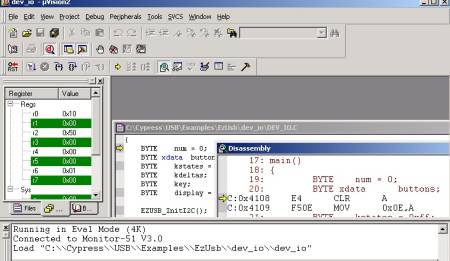
The Keil EZ-USB-FX environment is very similar to Microsoft Visual Studio
C/C++ development.
You see me single-stepping an example program. There is a pointer
to the C source and a pointer to the 8052 disassembly as instruction
execute.
Since csd does BASIC52, Forth, C, and assembler we emphasize that BASIC52
and Forth are operating systems.
BASIC52 is an interactive operating system written in assembler. BASIC52
compiles and/or interprets its own code on the '52.
Forth is an operating system written in Forth and Forth assembler.
Forth incrementally compiles and assembles its own code on a '52.
C is not an operating system. C is a compiled language.
In the case of the 8052, C is cross-compiled on a PC.
csd has printed the on-line Cypress manuals and errata sheets.
Stay tuned for later reports on the Cypress/Keil USB development environment.
There are many reasons that one wants to communicate from peripheral hardware
with a PC over USB 1.1 or 2 instead of
pci/cardbus. |
The new 8052 microcontrollers are essentially the equivalent of
Pentium-class processors in the embedded world.
Most new 8052 have two data pointers, operate at very high clock
frequencies, and only take several clocks per instructions compared with
the original 12 clock cycles per instruction.
Because of the 8051 family serial expansion bus instructions and
hardware, the 8051 family is ideally suited to usb2 and 1394
communications.
The problem now is of software, not hardware, for the 8052s. These
8052s need an interactive operating system to speed development of applications
software.
And they need to talk to windows 2000 applications through wdm 32
drivers.
This is csd's speciality learned at Sandia National Laboratories.
1
Wednesday January 24, 2000
07:02
The above announcement is from technology innovations, analog edition
page 23 Volume 7 February 2001 Texas Instruments
http://www.ti.com/sc/techinnovations7,
phone 1 800 477 8924, Suggested resale price state at $6.44 each in
1K qty. |
Because of USB and 1394 serial buses, wdm drivers will inextricably
be connected to new 80c52 software.
Note that Weiss's article didn't include the new Texas Instrument
TUSB 5152 which may run at 96 MHz with two clocks per instruction
cycle. Monday February 12, 2001
10:47
embedded hardwareupdates
By Ray Weiss Senior Technology Editor
8051 Keeps Plugging Away:
Faster CPUs, Smaller Packages
The 8051 8-bit microcontroller just keeps plugging away, adding new
peripherals, speed grades, and packaging. Among the latest advances is Dallas
Semiconductor’s 8051 implementation that delivers a 50x speedup over
the original 12-clock instruction execution implementation.
Another 8051 vendor, Cygnal Integrated Products Inc., is
fielding its own 20x speedup version of the 8051, coupled with a 12-bit
ADO. And on the size front, Philips Semiconductor has introduced an even
smaller 8051 package that targets deeply embedded applications.
8051s continue to be one of the more popular 8-bit microcontrollers.
Thousands of engineers and programmers know its ISA intimately.
Furthermore, there are tens of thousands of 8051 microcontroller programs
and function libraries available that remain in use.
Because of its rather baroque addressing scheme, the 8051 may not be
a super-easy architecture to use. But isn’t a simple, 8-bit microcontroller
with a restricted register easy to use? It has enough registers (2 banks
of 16 registers) and addressing to handle mid-size applications.
A 50x Speedup Dallas Semiconductor has made a good business of clean-room
8051 designs that push the 8051’s speed limits. Its newest version,
the D589C420, delivers a 50-MIPS, which is a 50x speedup over the old 1 2-MHz,
12-stage 8051. Running at 50 MHz, it executes an 8051 instruction in a single
clock cycle. Moreover, it offers a full redesign one that implements the
8051 ISA with modern RISC-like technology. The 8051’s sequential 12-stage
execution model was transformed into a 4-stage pipelined architecture that
delivers apparent 1-cycle instruction execution.
An ultra-high-speed microcontroller, the D589C420 is 100% pin- and
instruction-set compatible with the 8051.
When it was first designed, instruction execution was cut to 4 clocks
instead of 12. This redesign decreases that amount to 1 clock cycle (pipelined).
In addition to being 80052-compatible, the 8051 features 4 bidirectional
I/O ports, a 16-KB flash memory, and a 256-byte scratch pad RAM: It also
offers 3 16-bit timers and a 1-KB data SRAM for MOVX operations.
Peripherals include 2 full-duplex serial ports, a programmable watchdog
timer, and 13 interrupts (6 external).
Now in full production, the D5879C42 is priced from $10.10 in 25,000-unit
lots. Packages include 40-pin PDIPs, 44-pin PLOCs, and 44-pin TQFPs. The
chip is available in two temperature grades: 0 degrees C to 7000 and —40
degree C to 85 degree C.
An 8051 In A 20-Pin TSSOP Philips Semiconductor made its reputation in
the 8051 world with its small packages. The company’s most recent variation
comprises the 87LPC762 and the 87LPC764. This package crams a full 8051 with
peripherals into a 20-pin TSSOP that’s just 4.4 by 6.5 by 1.1 mm. It
cuts the 8051 packaging footprint by 1.3.
The 87LPC762/764 runs at up to 20 MHz and uses a 6-clock core (6 clocks
per instruction, not 12). It has 2 timer-counters, an 120 serial bus, a UART
serial port, and 2 KB or 4 KB of OTP memory, respectively. Plus, both
micocontrollers support power-on reset and a keypad interrupt. They support
12 interrupts (3 are extemal).
In 10,000-unit quantities, the 87LPC762 sell for $1.05 each, while the
764 is priced at $1.15 per unit. Both are packaged in TSSOPs.
A 20-MPS 8051 Plus A 12-Bit ADC Dallas Semiconductor is not the only 8051
vendor to re-implement the venerable 8-bitter for speed. Cygnal’s engineers
redesigned the 8051 as well, getting a 1-clock cycle (pipelined) instruction
execution. Its 8051 implementationruns at 20 MHz and delivers 20 MIPS peak.
Cygnal’s 08051 Fxx is a family of 8051-based mixed-signal, flash
memory processors. The 08051 F002 boasts a 20-MHz, 20-MIPS 8051 CPU with
32 KB of in-system programmable flash memory and 256 B of S RAM. Peripherals
incorporate a UART serial port, an SM Bus port, 4 8051 timers, and a 5-channel
programmable counter array. Among the mixed-signal peripherals are a 12-bit
ADO, 2 12-bit digital-to-analog converters, and a voltage comparator. Available
in 1000-unit lots, the 08051 F02 is priced at $12.13. The 08051F000DK development
kit costs $99.
Dallas Semiconductor, 4401 Beltwood Pkwy, Dallas, TX 75244; (972) 371-4000;
www.dalsemi.com.
Philips Semiconductors Inc., 811 E. Arques Ave., Sunnyvale, CA 94088;
(408) 991-2000;
www.philips.com.
Cygnal Integrated Products Inc., 4301 Westbank Dr., Building B, Suite
100, Austin, TX 78 746-6564; (512) 327-7088;
www.cygnal.com.
Electronic Design Feburary 5, 2001 page 93 |
Either or both usb2 or 1394 will likely become the standard way to
communicate with PCs in the future. Through wdm drivers, of course.
Macs apparently have 1394 installed on the motherboard.
Bergeron's article, reproduced at this site, predicts that usb20
will be standard, as usb10 is now, on motherboards within several
years.
It is quite likely, if not certain, that the MAXTOR 1394/FIREWIRE
PCI ADAPTER CARD seen below has a microcontroller on it. Also the disk
drive, too, has a microcontroller.
Fast 8051 family microcontrollers are a natural for either 1394 or
usb20 peripheral and bus interface.
Getting parts is a major concern with practical projects.
Chips can be placed on allocation.
Designing hardware with parts you can't buy is called designing with
unobtainium.
Having multiple sources for a designed-in microcontroller can be
a very important consideration if a company does not want to initially stock
as many parts as it intends to sell plus spares.
The 8051 family is unquestionably the most easily obtained
microcontroller.
The Maxtor product seen below uses Lucent technologies FW323
1 which
appears to be directly connected to the PCI bus.
Monday November 6, 2000
14:17
Advertisement by Staples, Albuquerque Journal Sunday November 5,
2000 |
The new 8052 microcontrollers are essentially the equivalent of
Pentium-class processors in the embedded world.
Most new 8052 have two data pointers, operate at very high clock
frequencies, and only take several clocks per instructions compared with
the original 12 clock cycles per instruction.
Because of the 8051 family serial expansion bus instructions and
hardware, the 8051 family is ideally suited to usb2 and 1394
communications.
The problem now is of software, not hardware, for the 8052s. These
8052s need an interactive operating system to speed development of applications
software.
And they need to talk to windows 2000 applications through wdm 32
drivers.
This is csd's speciality learned at Sandia National Laboratories.
1
Wednesday January 24, 2000
07:02
The above announcement is from technology innovations, analog edition
page 23 Volume 7 February 2001 Texas Instruments
http://www.ti.com/sc/techinnovations7,
phone 1 800 477 8924, Suggested resale price state at $6.44 each in
1K qty. |
Power consumption is becoming a major concern in the computing industry.
California's recent power problems high-lights this.
Windows 2000 wdm drivers have extensive power management hooks in
them.
80C51/52 microcontroller have two power down modes. This makes the
'C52s [8051's are largely obsolete] a good choice for peripheral hardware
controllers.
The power consumption of a 'C52 is roughly linear with the clock
speed. Therefore those new fast 'C52s must be placed in a low-power
state when the wdm driver sends a message relayed from windows 2000 that
inactivity can be expected.
usb power cable only supplies 150ma of power too.
Bill Gates understands the PC power problem and, apparently, wishes
to make more money from it.
Friday February 2, 2000 09:59
Bill Gates buys a hefty hunk of PNM
Bill Gates adds 2.3 million shares of PNM to his portfolio
BY ROSALIE RAYBURN
Journal Staff Writer
Billionaire Bill Gates, an Albuquerque resident when he started Microsoft,
has become the second-largest shareholder in Public Service Company of New
Mexico.
Cascade Investment LLC, the company that handles the Microsoft
chairman’s personal portfolio, announced this week it had bought 2.3
million shares of PNM. —
"When the richest man in the world shows interest, it’s
flattering,” utility 2.3 million spokesman Bob Hagan said:
The deal gives Gates a 6 percent stake, making him the second-largest
investor after Prudential Investments, Hagan said.
About 70 percent of PNM share are owned by institutions.
“We were aware several weeks ago that Cascade was accumulating stock,
but we don’t know what their motivation is, "said Hagan adding that
the deal doesn’t give Gates a controlling interest in PNM.
Cascade disclosed the deal in a filing Monday with the U.S. Securities
and Exchange Commission.
Analyst Joan Goodman of Pershing, a division of Credit Suisse First Boston,
said what could make PNM attractive for Gates is that the company's price
is relatively low but has been moving up. Earnings are up 21 percent and
utilities throughout much of the West except for California have been doing
well because of high power prices.
PNM stock, trading at about $15 last year at this time, closed Wednesday
just under $25.
“When someone like Gates takes a position in a company, it's always
positive,” Goodman said.
Cascade, of Kirkland, Wash., began its buying spree shortly after PNM
announced plans to buy Western Resources, a Kansas utility, in November.
Gates has been showing an interest in the power sector in the past year.
Earlier this month, Cascade bought 5.01 percent of Avista Corp., an electricity
and gas company based in eastern Washington.
And last June, Cascade bought an additional 235,000 shares of Otter Tail
Power Co., bringing its total investment in the Minnesota utility to $25.2
million.
Other major institutional shareholders in PNM include Donald Smith &
Co. (5.12 percent), Barclays Global Investors (4.34 percent) and Colonial
Management Association (3.37 percent).
Albuquerque Journal, Business Outlook, Thursday February 1, 2001 |
Basic52 is a
basic
interpreter written by Chandler Arizona Intel employee Tom Katausky in
the 1980s.
Style of the Basic52 interpreter technology is much the same as that
used by Bill Gates to write his BASIC for the Altair and Microsoft Corp,
IBM Personal Computer.
BASIC styles vary enormously. The Sinclair ZX-80/81 was written
in a byte-coded technology similar to Java.
CSD possesses the source code for Basic52 and floating point extension.
We'll eventually post this code at this web site.
CSD has written and debugged 8051 assembler modules in Forth assembler.
The debugged assembler modules are then included with Basic52 application
program.
Basic52 systems are included in many commercial products.
Cost of software development on either a Basic52 or Forth development
system are order of magnitude less expensive than on cross development platforms.
The 8051 becomes its own development system.
Practical experience has shown that both Basic and Forth system are
more reliable in the field than those written in other software technologies.
One reason may be that both are very simple software
technologies.
Wednesday July 19, 2000
19:50
8051-based hardware makes a fine software buffering system ... as
opposed to hardware fifos ... to a wdm driver. Also to perhpheral analog
and digital hardware.
8051 is a generic term.
Most new 8051 microcontrollers incorporate the 80c32 instruction
set. 5 means the part has an internal rom.
3 means no internal rom. However, parts overages in custom
5 parts are sold as 3 parts.
Two interactive real-time operating systems are available for
8051 family microcontrollers.
BASIC 51 and
Forth.
"real time" means that interrupts are never disabled within the operating
system. Wednesday July 19, 2000
19:46
| Mentor Graphics Corp. (Wilsonville, Ore.) has announced the M8051E-Warp--a
high-performance, user-programmable 8051-based 8-bit microcontroller with
a built-in chip debug feature.
The M8051E-Warp Uses on-chip instrumentation (OCI) technology developed
in collaboration with First Silicon Solutions (Beaverton, Ore.) to provide
a JTAG-based debug solution.
The OCI, working in concert with in-circuit emulation tools, enables
engineers to run at-speed validation of a system-on-chip and application
program. The company claims that application developers can perform simultaneous
application development and validation on a hard ware platform based on multiple
third-party IP. In addition, application developers gain comprehensive real-time
control of the processor from a PC-based interface with access to step, trace,
soft breakpoints, hardware triggers and read/write control of registers and
memory.
The core has a frequency-scalable state machine, is silicon-proven at
120 MHz and uses 0.18-micron process technology. Mentor said it can surpass
50-Mips performance reliably, uses only two clocks per instruction cycle
and achieves six times the performance of a standard 8051 core at the same
power consumption while maintaining full functional compatibility with legacy
devices.
Mentor ships the M8051E-Warp soft core with sample synthesis and scan
insertion scripts, a functional test bench with over 99 percent coverage
and complete product documentation. The M8051E-Warp soft core is available
now. Visit
http://www.mentor.com/inventra/
Edited by Michael Santarini
Electronic Engineering Times July 17, 2000
http://www.eet.com/ |
Improperly asserting 8051 family reset causes a Forth or Basic52
operating system and applications codes to crash.
Another of the 8051 family processors distinquished attributes is
its two low power states.
Countless applications involve a µC which
sleeps to conserve power until awakened by some external alarm
circuit.
Emerging from either low-power state is tricky.
Hopefully Chrzaszcz's circuit works well. For this is a very
important circuit.
C or C++ are languages. They are not operating systems.
Therefore, a development system with an emulator is usually required
for software development using these languages.
Engineers and programmers in many foreign
countries cannot afford a µC development system and don't
need one.
Therefore, Forth and BASICs are used extensively outside the United
States. Sunday July 23, 2000
08:40
| Use 8051's power-down mode to the fullest
Jerzy Chrzaszcz, Warsaw University of Technology, Poland
THE 8051 SERIES µCs offer idle and power-down modes, both of which
you invoke by setting appropriate control hits from the code. For instance,
a 5V, 12-MHz Atmel AT89C2051 consumes approximately 9 mA in active mode,
1.8 mA in idle mode, and only 12 µA in power-down mode. Although power-down
savings outperform those of the idle mode by two orders of magnitude, the
only way to restore the AT89C205l’s operation from a power-down state
is to reset, which constitutes a serious drawback for system designers. This
disadvantage holds true for most 8051-compatible processors; only high- end
models wake from power-down state by interrupt. However, a simple method
exists for using an ordinary 8051 in power-down mode with interrupt recovery.
You can easily adapt the proposed solution for various requirements; the
only assumption is that an external device, such as a keyboard or sensor,
asserts an interrupt request, which is negated when the processor takes a
specific action, such as reading the status register. When the µC has
nothing to do, the program switches the external pin on the µC low,
and the µC enters power-down mode.
The incoming interrupt request passes through the NOR gate (Figure la),
causing a processor reset (Figure 1b). When the port pin is automatically
high, the gate closes, negating the reset signal. Such a scenario requires
an initialization program to distinguish between cold restart (power-up)
and warm restart (wake-up).You can easily accomplish this function by checking
whether locations in data memory match a predefined pattern (signature),
which is set just before entering power-down mode. For details on the
warm-restart concept, refer to application note AN424, “8051 family
warm boot determinations” from Philips. Another problem is restoring
special-function registers’ contents—unlike internal data RAM,
which remains unchanged, Special-function registers are automatically initialized
upon reset. Depending on the application, some registers may always be set
to predefined values, and some must be stored in data memory before entering
power-down mode and reloaded during warm restart. You can download the necessary
software listings from EDN’s Web site,
http://www.ednmag.com/. Click on
“Search Databases” and then enter the Software Center to download
the file for Design Idea #2557. (DI #2557)
EDN July 6, 2000 |
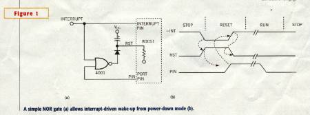
|
Forth and BASICs are operating systems. Not just computer languages
like C.
Failure to have an operating system on a microcontroller means that
a cross-development system and emulator must be used.
The C8O5lFxxx parts have built-in emulation circuitry that communicates
with an integrated development environment, eliminating much of the external
emulation hardware required with many MCUs. The device on the target board
connects to an emulator cartridge that is about the size of a deck of cards.
The cartridge links via an R5232 serial port to a personal computer, which
runs the editor, a macro-assembler that works with any C-compiler, and a
debugger.
The C8O5lFxxx parts have built-in emulation circuitry that communicates
with an integrated development environment, eliminating much of the external
emulation hardware required with many MCUs.
The device on the target board connects to an emulator cartridge that
is about the size of a deck of cards. The cartridge links via an R5232 serial
port to a personal computer, which runs the editor, a macro-assembler that
works with any C-compiler, and a debugger.
Wdm drivers will be required to communicate between Windows 98, Me,
and 2000 and these microcontrollers.
These specialized 8051s require purchase of enough parts for about
all expected sales and replacement parts.
Reason is that these parts can be discontinued and you're left to
redesign your product around some other part!
Wednesday August 9, 2000 13:53
Cygnal SoC pushes 8051 speed
By David Lammers
AUSTIN, TEXAS — Cygnal Integrated Products Inc. is ready with its
first system-on-chip ICs, which push the speed of an on-chip 8051 processor
core to 20 Mips while adding high-performance analog that is configurable
as opposed to programmable.
Cygnal, a startup based here, has roots in mixed-signal technology. Chief
executive officer Derrell Coker founded Benchmarq, the smart-battery IC company
bought by Texas Instruments Inc. Doug Holberg, Cygnal’s chief technology
officer and vice president of engineering, was a founder of Crystal Semiconductor
Corp. He and marketing vice president Don Alfano, had also worked at Mostek
(Dallas) in the 1970s.
Though the configurable analog capabilities are their main feature,
Cygnal’s first products are based on a pipelined 8051 code-compatible
core that is faster—at 20 Mips peak on a 20- MHz core—than anything
on the market, Alfano said. About 70 percent of the instruction set is
single-byte.
Alfano said that he analog on the 8051-based offerings on the market
has been significantly inferior. Some companies claim “programmable”
analog, which Alfano said implies that the analog can be anything. “We
call ours configurable, meaning that we can change certain characteristics
by 5 to 10 percent so that the user can tune it," he said
Holberg said, "What we have is an analog-to-digital converter that can
be switched on the fly, on a channel-by-channel basis. And it can be switched
from single to differential input mode. With other parts, if you want to
do that you need external components on the board.
“Besides the flexibility,” said Holberg, “we believe the
performance of our on-chip analog is unmatched: we have used innovative circuit
and noise management tricks in our mixed signal that no one else has accomplished
in a field-programmable part.”
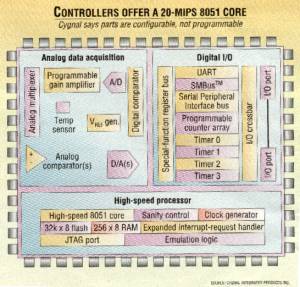
The Cygnal parts meet the needs of industrial control systems where switching
among multiple channels is critical. A system measuring temperature, flow,
humidity and pressure must be able to measure those multiple channels and
then perform mathematical operations before outputting the data to hardware.
Those environments require analog circuitry that can filter out ambient noise
and perform filtering on offset or gain-corrected signals.
Cygnal uses a 0.35-micron process at Taiwan Semiconductor Manufacturing
Co. (TSMC; Hsinchu, Taiwan) that is optimized for mixed-signal and flash
capabilities. Cygual’s products include 32 kbytes of in system-programmable
flash, specifically the split-gate flash cell from Silicon Storage Technology
Inc. (Sunnyvale, Calif.), which is optimized for the TSMC process.
Also, TSMC's mixed-signal module includes a double-poly layer that Holberg
said supports the ability to do precise on-chip capacitors with a better
ratio of desired capacitance to the parasitics. “And the resistors,
because of the poly and a tungsten silicide, are higher-valued resistors,
at about 100 to 200 ohms per square,” he said. Cygnal’s initial
products offer either 10- or 12-bit A/D converters with 100 ksamples/second.
Gain can be adjusted from 0.5 to 16, and the eight inputs can be configured
as four pairs of differential inputs. The inputs can be mixed and matched
under program control.
“The differential comparator feature that we have is a major difference
with our products, Holberg said. “Another is a crossbar switch that
allows the designer to assign the peripheral circuits to certain functions.
Analog Devices also offers a crossbar, but we believe ours is much faster
than the uC812 parts from ADI.”
An IDA in the palm of your hand
Holberg said many of the 30 or so employees at Cygnal are mixed-signal
engineers who worked with him at Crystal, which he co-founded with Mike Callahan.
Another group came from Intermedics when it closed a design center here.
Founded in March 1999, Cygnal took about 16 months to finish its first
MCUs,which cost about $10 to $12 in thousands of units. The devices themselves
are only part of the story.
The C8O5lFxxx parts have built-in emulation circuitry that communicates
with an integrated development environment, eliminating much of the external
emulation hardware required with many MCUs.
The device on the target board connects to an emulator cartridge that
is about the size of a deck of cards. The cartridge links via an R5232 serial
port to a personal computer, which runs the editor, a macro-assembler that
works with any C-compiler, and a debugger.
The development kits can ordered from
http://www.cygnal.com/ at a cost of
$99. Coker said about 100 engineers who helped define the product were given
free development kits, and he claimed that 30 of them are actively designing
products.
Electronic Engineering Times August 7, 2000
http://www.eet.com/ |
|
|
Another 8051 specialty chip.
Monday September 4, 2000 08:44
Forth and Java are very similar. In fact, the Sinclair ZX80/81
were implemented in a byte coded threaded technology.
The RTX 2000 runs Forth mostly in hardware.
Primary difference between 'normal' processors is that a Forth chip
has two hardware stacks. The 'data' stack and the 'return'
stack.
The RTX 200 is also very simple. Therefore it it naturally
radiation hardened.
http://www.cs.cmu.edu/~koopman/stack_computers/sec4_5.html
http://dec.bournemouth.ac.uk/forth/rfc/rfc88.html
http://www.elilabs.com/~rj/dreams/node28.html
Russians use Forth technology. Even for fuzing weapons
systems.
http://www.koenig.su/win/cherezov/forthcpu/forth32.html
Because of the much greater software reliability of Forth technology
[it doesn't crash as much as other operating systems], this is an ideal
technology for use where one can't easily access the hardware. In space
and under water.
http://forth.gsfc.nasa.gov/
While Forth is execellent for stability reasons, it executes
high-level code at about 10% the speed of assembler or C code. Java
is even worse.
Forth, however, is an ideal interactive real-time operating system
for an 8051 family microcontoller.
http://www.elecdesign.com/magazine/1999/nov2299/embed/1122es1.shtml
Speed-critical code can be recoded from high-level into machine code
using Forth interactive incremental assembler.
Monday September 4, 2000 08:44
| WOLFE’S DEN by ALEXANDER
WOLFE
Java chips in comeback?
On the cusp of the embedded Systems conference/Fall, to be held next month
in San Jose, Calif., the most interesting item swirling around the embedded
market has been the refusal of Java. chips to up and die. Despite much talk
and even some legitimate evidence that they're heading in that direction.
Sure, Sun Microsystems bid to build silicon that would execute Java directly
in hardware cannot really he considered a success. The company has fared
much better away from the embedded arena. Indeed, Sun, along with IBM Corp.,
has become a top player in taking Java software into enterprise computing.
Meanwhile , embedded Java devices (including offering from NEC and Fujitsu)
appear to have languished for lack of interest.
Now, however, Java silicon seems ready to heat up again. A major case
in point is Agile Systems, which has
just inveiled its JEM2 direct-execution Java processor (see Aug. 21, page
79). The chip arose from work originally done at Rockwell-Collins several
years ago. Though that company declined to take JEM commercial, a dedicated
group of engineers within Rockwell spun out Agile and got the job done.
Many insiders believe there are other Java chips from other vendors in
the wings poised to hit the market this fall. Already, LG Semicon has weighed
in with a vigorous offering, which includes a reference design for a set-top
box. Patriot Scientific
Charles Moore, Forth's inventor wrote the Shboom compiler
has long sold a Java device.
“I think you’ll wind up seeing more Java implementations in
silicon shortly,” Doug Higgins, president of embedded Java software
house Newmonics Inc. (Lisle, Ill.), told me recently. However, as those cryptic
words indicate, it a still not clear exactly which companies will be fielding
the chips. More information should be forthcoming next month at the embedded
conference.
The impetus for all this activity is the broadening need for low-power
and mid-level-performance devices, at a decent price, which can power a new
generation of Internet appliances. Now, the big question is, how will Intel
Corp. respond?
Will the microprocessor giant remain content to sit on the server side
of the network equation or will it move to expand its offerings beyond the
Strong-ARM processor (still a high-end part) and delve into the low-power,
deeply embedded market? Intel certainly has the technical wherewithal to
do so, but so far is showing no signs of going down that road.
August 28, 2000 Electronic Engineering Times
http://www.eet.com/ |
The 8052 makes a fine candidate to communicate through a Windows
wdm driver to a Windows application program
Thursday August 31, 2000 10:14
These 8-bit microcontroller need to talk to windows through wdm
drivers. Wednesday September 20, 2000
13:04
| Revamped 8-bit MCU still attractive to portable designers
Added functionality and better development support extends the life
of 8-bit MCUs.
Anita S. Becker, Technology Editor
The old workhorse of the portable world, the 8-bit microcontroller unit
(MCU), is far from being put out to pasture. Instead it's being groomed for
additional duty. Popular for almost two decades because of its low-cost chips
and compact code size, the 8-bit MCU now offers designers easier-to-use,
C-based development tools; on-board nonvolatile memory; increased performance;
and more on-board peripherals. ....
More memory
Over the past 18 months flash memory has popped up all over the 8-bit
MCU landscape. Silicon Storage Technology (SST—Sunnyvale, Calif.) recently
announced an enhanced version of its SuperFlash-based FlashFlex51 family
of 8-bit, 8051-compatible microcontrollers. SST's new family includes the
SST89C54, incorporating 20 kbytes of integrated on-chip flash memory, and
the SST89C58, with 36 kbytes of integrated on-chip flash memory. Originally
introduced in 1999, both products have been enhanced to include additional
power-saving features, improved in-application programming (IAP) capabilities,
and extended security modes.
Both products leverage SST's proprietary SuperFlash technology, which
uses a small sector size for both code and data storage, and is aimed at
high-volume applications. A major enhancement to the FlashFlex51 is in the
IAP technology. SST developed an architecture wherein the flash memory is
mapped into two independent banks. This dual-memory bank architecture results
in an IAP mode that allows the CPU to run user programs from one bank to
the other while concurrently servicing a flash programming operation in the
background on the other bank.
The company also improved the CPU core of the FlashFlex51 devices, resulting
in a power-saving mode that features a wake-up-with-interrupt, with no loss
of program sequence prior to power down. In this new mode, the clock is stopped
and current dissipation is reduced to 15 µA, yet interrupts are still
active. This feature is aimed at portable, battery-power-sensitive applications
such as handheld scanners, personal digital assistants (PDAs), and electronic
games.
Where is the 8-bit going?
"Not surprisingly, connectivity is really the big thing that we're seeing
customers require," says Doug Davis, general manager, Intel's Embedded
Microcontroller Division (Chandler, Ariz.). "What that means is the ability
to take some device that's using an 8-bit controller and using that device
to communicate over the Internet." Intel's 83C51KB, part of the MCS-51 family
of 8-bit MCUs, can be found in applications such as stand-alone keyboards,
small hard-disk drives, and in laptops, but currently isn't equipped to perform
this function.
Many manufacturers are seeing a demand for microcontrollers that can support
communications interfaces such as Bluetooth, Ethernet, and others. Although
primarily in the domain of higher architecture microcontrollers such as the
32-bit and beyond, in the near future, producers of high-end, higher frequency
8-bit MCUs will be able to offer such devices for certain applications such
as networked appliances. But, most likely, the role of the 8-bit MCU will
be a supporting one. It will be more efficient for designers to use 32-bit
and higher MCUs for most Internet connectivity applications.
"My expectation is that 8-bit microcontrollers will be around for a very
long time," asserts Intel's Davis. "To me, the defining line that will determine
what requires an increase in performance to 16 bits or higher is really going
to be that connectivity piece. There are some things that are a dedicated
function today, and for the most part will remain a dedicated
function—that's where the 8-bit is. Once it's networked, you have to
go up in speed. Without the communications piece there's always a segment
of the market that will remain 8-bit."
1
Portable Design
http://pd.pennnet.com/home/home.cfm
September 2000 |
These fast 8051 may be the ideal peripheral controller for usb20
or 1394 communication to Windows 2000 wdm drivers.
Fast, inexpensive, available from multiple vendors, operating systems
available for them.
Saturday November 4, 2000
10:15
| 8051 microcontroller core hits 50 Mips
DALLAS — The latest redesign of Dallas Semiconductor’s 8051
processor core has produced a microcontroller that’s able to execute
one instruction per clock cycle at 50MHz, equivalent to 50 Mips.
Microcontroller product manager Frank Taylor said the DS89C420 runs 50
times faster than the original 8051. The current-generation part features
16 kbytes of flash memory with in-system, in-application and standard flash/
EPROM modes.
An on-chip boot loader opens the flash for access via the serial port
when the DS89C420 is operating in its in-system mode. Taylor said the DS89C420
can be assembled and shipped “erased” and then programmed on-site
for application-specific purposes. It can also be used to replace an older,
8051-type controller, for a substantial performance gain.
In the in-application mode, the on-chip memory management unit alternates
memory blocks, so that application software can execute in one block while
the other is erased and programmed.
Taylor said that despite speed approaching that of RISC chips, the DS89C420
remains pin- and instruction- set-compatible with existing 8051-based systems.
To account for differences in processing speed, the controller provides a
stretch-cycle feature and page or nonpage memory interface modes to enable
communication with slower external memory and peripherals.
Dallas’ first redesign of its 8051 core reduced the number of clock
cycles per machine instruction from 12 to 4. “We still wanted to break
limits, however, so we overhauled the design again,” Taylor said. The
maximum crystal speed jumped to 50 MHz from 33MHz.
“It potentially takes several RISC instructions to achieve the same
result as one 8051 instruction,” Taylor said. “The DS89C420 has
the power of the full 8051 instruction set.”
The controller includes two data pointers that can be used to move blocks
of data forward and backward with fewer instruction steps, for faster
operation.
Other features include 13 interrupt sources, with five priority levels
instead of three; three 16-bit timer/counters; and a watchdog timer. An internal
clock divider circuit enables power management mode, in which the DS89C420
selects a processing speed based on software input and maintains all processes
at lower-power states without shutting down. A clock multiplier allows full-
speed operation from lower-speed crystals that are more readily available.
The DS89C420 is sampling now; production availability is scheduled for
January. It will be priced at $10.10 in quantities of 25,000. Call (972)
371-3832 wwwdalsemi.com
Electronic Engineering Times October 30, 2000
http://www.eet.com/ |
Wdm drivers will be required to communicate between Windows 98, Me,
and 2000 and these microcontrollers.
These 'specialty chips' may require purchase of all that are needed
for a product's life time. Frequently, no more a made.
Saturday November 4, 2000 10:15
| Atmel 80C51 MCU packs A/D on board
SAN JOSE, CALIF. — Atmel Corp.’s wireless and microcontrollers
unit, based in Nantes, France, has introduced a line of 8-bit, 80C51
microcontrollers with a 10- bit, eight-channel analog-to- digital converter
plus a programmable dual-clock system that’s said to allow advanced
mastering of speed and power consumption.
The T8xC5111/12 also includes a programmable counter array for pulse-width
modulation, capture/compare, timers, counters and watchdog capabilities,
as well as a serial peripheral interface. Parts operate at 66 MHz at 5 volts
or 40 MHz at 3 V.
Manish Vadher, marketing director for microcontrollers, said the MCUs
are aimed at industrial control and consumer appliance applications in which
low power consumption and a minimal components count matter.
The dual system clock and one timer allow real-time clock functions at
32 kHz. The clock includes a 12-MHz RC oscillator and a programmable prescaler,
and it’s said to work with either a reference crystal or a 32-kHz or
4- to 33-MHz ceramic oscillator.
The integrated AID has an internal 2.4-V positive-voltage reference and
can also accept an external positive voltage ranging from 2.4VtoVcc. The
voltage reference can be used externally to reduce the need for another
component.
The T8xC5111 and T8xC5112 include 4 kbytes and 8 kbytes of ROM or OTP
memory, respectively, as well as 256 bytes of RAM. Secured ROM check is available
with a 64-byte encryption array and three security levels.
T8xC5111 devices are available in 16-pin SSOP, 24-pin DIL or 24-pin SO
packages with 201/Os. T8xC5112 versions, with 401/Os, are available in 52-pin
PLCC or 48-pin LQFP packages. Commercial and industrial versions are offered.
Prices start at $1.50 each in quantities of 100,000. Call (408) 441-0311
www.Atmel-wm.com
Electronic Engineering Times October 30, 2000
http://www.eet.com/ |
Windows 200, 98, ME wdm would speed peripheral software development.
And permit source code to be both compiled and assembled on the 80C32
processor Friday April
28, 2000 16:41
| USB 2.0. with 480-Mbit transfer rate, is set to
roll
By David Lammers
SAN JOSE, CALIF. — The final Universal Serial Bus 2.0 specification
is expected to be released this week at the Windows Hardware Engineering
Conference in New Orleans, and become available on the USB Implementers Forum
Web site (www. usb.org), EE Times
has learned.
The release is expected to kick off a wave of silicon supporting USB
2.0, which extends the fullspeed transfer rate from a possible 12 Mbits/second
in USB 1.1 all the way up to 480 Mbits/s.
The firstsystems usingthe 2.0 specification are expected to debut for
the Christmas PC selling season, and a number ofcompanies are expected to
announce 2.0 silicon at the USB Developers Conference, planned for May 15-17
in Anaheim, Calif.
NEC Corp; took an early plunge in mid-April, unveiling a 2.0 host controller
that supports the full 480-Mbit/s data transfer rate. NEC is sampling the
device this month and plans to begin commercial production in September.
NEC's host silicon is backward compatible with the full-speed USB 1.1 standard,
incorporating two USB 1.1 host controllers that will double the 12-Mbit/s
speed limit of peripherals conforming to the USB 1.1 specification.
The physical layer on the NEC controller supports the full 2.0 transfer
rate, and can dynamically configure the bandwidth according to the speed
capabilities of the connected devices, an NEC spokesman said.
The USB initiative has enabled far simpler connections of peripherals
to personal computers, compared with serial ports or SCSI links. Because
the connections can be made while the host system is up and running, USB
has been one of the true success stories in making PCs easier to use.
Jason Ziller, an Intel Corp. manager who heads up the USB 2.0
promoter’s group, said the new spec, with data rates of 60 Mbytes/s,
is about 40 times faster than the USB 1.1 specification.
The higher bandwidth will enable applications such as interactive games
and digital image creation, and’will be used in scanners, printers,
external storage devices and broadband Internet connections. A gigabyte of
data can be backed up in less than a minute to an external drive with USB
2.0, for example. Also, a high-density flash card containing dozens of
high-resolution images can be downloaded from a digital still camera to a
computer in a matter of seconds, Ziller said.
The emerging field of Internet appliances is also leaning on USB. A network
appliance being developedhy IBM Corp. has seven USB ports, one source said.
The 2.0 spec calls for the same cables and connectors used in the 1.1
standard,butthevoltage swing in the controllers has been cut to 400 millivolts,
from 3.3V in the version 1.1 USB chip sets. Also, dual termination is required
on both ends of the wire.
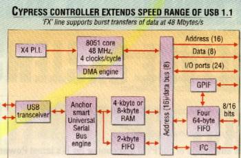
While the first generation of 2.0-enabled systems is expected to stick
with the 480-Mbps transfer rate, some companies already are planning to push
the 2.0 specification higher, according to one source, who asked not to be
identified. But that won’t happen until well into 2001, when 2.0 is
expected to graduallysupplant the 1.1 specification.
To help bridge the gap, Cypress Semiconductor Corp. has developed aline
ofUSB 1.1 controllers that supportburst transfers of data, typical in storage
or video cameras, at up to 48 Mbytes/s—not much slower than the 2.0
limitof 60 Mbytes/s. The “FX” (faster, extended) line builds on
the basic architecture of the Cypress 8051-based EZ USB controllers, which
are based on technology gained in the May1999 acquisition of Anchor Chips,
a San Diego-based fabless USE company.
That acquisition, and a deal to acquire Intel’s USB silicon operation
last year, put Cypress in the lead in terms of USB silicon sales. The San
Jose company expects to ship about 16 million USB controllers this quarter,
saidAllyn Pon, aformer Anchor executive who is now marketing director of
the interface products division at Cypress.
The FX line of USE host silicon provides a migration path to the 2.0
spec, Pon said. The seven parts in the line are sampling now and go into
full production in July, priced in the $7 range.
Pon said the FX controllers support the 16-bit transfers needed for
mass-storage peripherals, as well as for the Phone Networking Alliance standard.
Timing is programmable. Direct memory access to external memory can buffer
up to 64 kbits of data, needed to sustain the USE transfer rate in bursty
applications. The FX silicon shaves packaging costs by using a plastic quad
flat pack with fewer pins than needed for the 2.0-compliant silicon, Pon
said
Electronic Engineering Time April 24, 2000
http://www.eet.com/ |
The 8051 microcontroller - actually now an 80C32 - is effectively
a public-domain microcontroller design which serves as a core to add on-chip
peripherals.
The software challenge is to implement subsets of the ieee 802.x
protocols to connect wdm drivers to 80C32 drivers which use the link layer
protocol hardware on these new chips.
Just as Visual Basic 6.0, Visual C 6.0, and DriverStudio 2.1 and
.5 provides an about interactive development environment for wdm drivers,
an interactive operating system on the 80C32 peripheral side would speed
software development.
More on how to do this later.
This has been done before at Sandia National Laboratories which builds
the 8051 as a radiation-hardened part for weapons applications.
Sunday April 23, 2000 10:00
| Cypress’ controllers to support USB
2.0
By DARRELL DUNN
Cypress Semiconductor Corp. is expanding its USB-controller portfolio
with a high-performance family that is expected later this year to support
the emerging USB 2.0 specification.
The new family cements Cypress’ position as the leading USB supplier
and marks an important milestone on the way to high-speed USB transmission,
according to Dave Podsiadlo, USB product marketing manager at Cypress in
San Jose.
“We finally have achieved critical mass of the installed base of
USB-enabled PCs,” Podsiadlo said. “There’s long been talk
about a killer application to put USB on the map, but it’s been basically
a whole plethora of applications that has led to the success. There are a
lot of players and a lot of choices for customers, and the challenge for
ourselves is that all those applications have different interface
requirements.”
The EZ-USB FX family of USB controllers Cypress is unveiling today are
capable of attaching to virtually any peripheral system, including mass storage,
home-phone network alliance (HPNA), wireless LANs, video, DSL and cable modems,
scanners, and printers, Podsiadlo said.
Demand for USB-enabled peripheral devices will grow from about 100 million
this year to 500 million in 2003, according to Dataquest Inc., San Jose.
The FX family expands the performance and capabilities of the EZ-USB
family Cypress introduced last year following its acquisition of Anchor Chips
Inc.
The FX family increases the 8051 microcontroller core’s performance
from 24 to 48 MHz, and adds direct memory access (DMA), internal FIFOs, and
a general programmable interface (GPIF). The controller’s smart-interface
engine handles much of the low-level USB logic overhead, simplifying the
8051 code and freeing the processor to service specific applications. Cypress
said.
The GPIF can be configured gluelessly to interface with ASICs, DSPs,
or standard interfaces such as Atapi, Utopia, enhanced parallel-port wireless
LANs, and HPNA chipsets. Internal FIFOs can be configured to an 8- or 16-bit
data path and allow master or slave operation, while the DMA engine transfers
data between the peripheral interface and external buffer memory. After the
FX controller has transferred data into buffer memory, the peripheral subsystem
can then fetch new data, Podsiadlo said.
The controller can move DMA packet data from external buffer to USB,
maintaining maximum USB performance even when the peripheral subsystem is
idle, he said.
The first offerings in the FX family will comply with the existing USB
1.1 specification supporting 12-Mbit/s peripheral speeds. Cypress plans to
introduce devices by year’s end that will support the emerging USB 2.0
specification for up to 480-Mbit/s performance.
The CY7C646xx family is sampling, with volume production to begin in
May. Cypress will offer seven versions with RAM, data-rate, program-I/O,
address-bus, and ISO support. The devices are priced between $6.88 and $8.13
in l,000s
Electronic Buyers New April 17, 2000
http://www.ebnonline.com/
|
| Cypress Semiconductor Rolls USB
Microcontrollers
CYPRESS SEMICONDUCTOR Corp. today will announce plans to sample a line
of 48MHz Universal Serial Bus (USB) microcontrollers that the company says
it will position for deployment into mass storage, wireless local area networks,
video, digital subscriber line equipment, cable modems, scanners, and printers.
Dubbed EZ-USB FX, the product family expands upon previous generations of
Cypress USB microcontrollers by adding faster input/output, direct memory
access, internal FIFO’s, and general programmable interface. The company
said interfaces to the part can be configured to be glueless to ASICs, digital
signal processors, or standard interfaces, such as ATAPI, UTOPIA, or EPP
(enhanced parallel port), wireless local area network chipsets, and HomePNA
chipsets. The internal FIFOs can be configured to an 8-bit or 16-bit datapath
and allow master or slave operation. The company said the part also lays
the groundwork for Cypress microcontrollers to meet the USB 2.0 standard
when it is approved later this year. The target data transfer speed for USB
2.0 is 480bits/sec., or about 40 times the speed of the current USB 1.1 standard
that transfers data at l2Mbitslsec. The products are sampling nov. with
production volumes expected by July. The family includes seven different
parts in packages of 52 PQFP, 80 PQEP, and 128 PQFP. The parts will be priced
from $6.88 to $8.13 each in lots of 1,000.
Compiled by Arik Hesseldahl
Electronic News April 167, 2000
http://www.electronicnews.com/ |