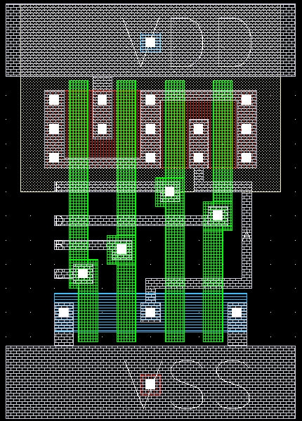
It is very difficult to draw the layout for complex logic gates without a stick diagram.
This symbol not only indicates the logic of the device, but also the relative location of each FET. Input B is "top of the stack" with respect to input C. The same can be said with input E relative to input D.
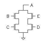
At the same time, the B/C path is "top of the stack" with respect to the E/D path.
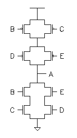
This transistor level diagram is valid for the above logic gate. With this schematic, the stick diagram can be generated.
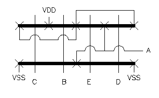
Once the stick diagram has been created, generating the layout is possible. First, draw the N-FETs, while remembering to follow minimum design rules.
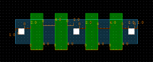
Gate C and B are 4 microns apart, as are E and D. All the channels are 8 microns tall and 4 microns wide because the schematic symbol indicated that was the size to use.
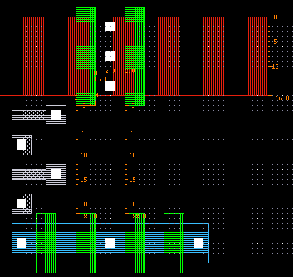
In this complex logic gate, there are contacts between each P-FET. This will make the total P-type diffusion much wider then the N-type. In an attempt to keep the polysilicon as straight as possible, P-FETs B and E should be lined up with their N-type counterparts.
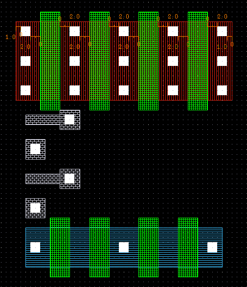
The center gates are lined up, and the contacts between them have been added. Following contact and polysilicon rules will permit the generation of the rest of the P-FET layout.
Now the metal enclosure of contact, and the routing can be made. On nodes where more then one contact exists, some contacts can be removed to make routing room.
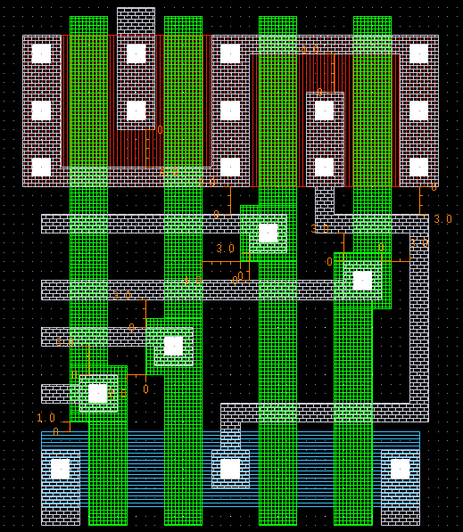
The last step is to add the power bus, taps, and label the inputs and output.