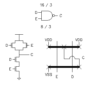
The layout for a NAND gate is done basically the same way. The only difference is that now there are two FETs per diffusion instead of only one.
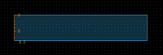
This NAND gate has a P-FET W/L value of 16/3, and a N-FET W/L value of 8/3. To start drawing this device, again start with the N-type diffusion.
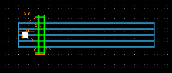
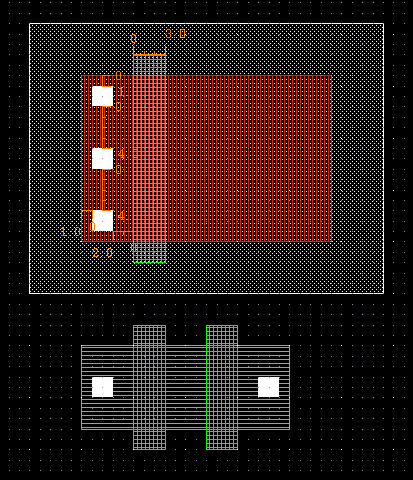
Now the contact and first gate should be created.
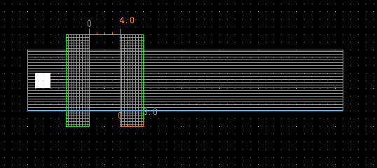
The second gate must also be drawn. Even though the minimum active size is 3 microns wide, the minimum gate to gate space is 4 microns. Therefore the second gate must be 4 microns away.
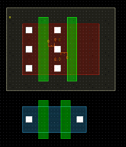
The N-FETs simply need the output contact, and then the P-FETs can be created.
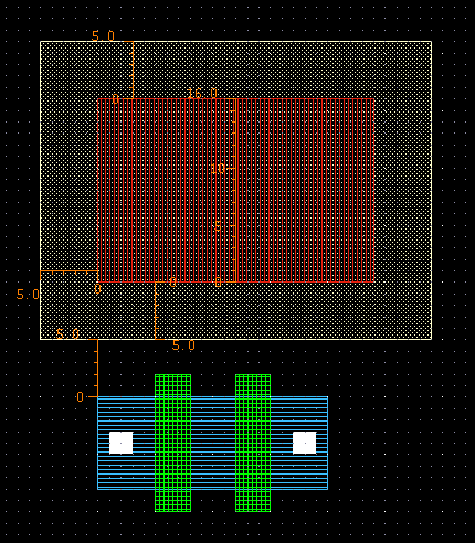
The N-Well is 5 microns away from the N-FETs, and the P-FETs are enclosed by the N-Well by 5 microns. The stick diagram indicate that there is a VSS and VDD lined up under each other. If possible, power nodes should be over top of each other. That way, power nodes between devices can be shared.
Because of how large the P-diffusion was, it was possible to add more then just one contact . When there is room, extra contacts should be added. The polysilicon must be 2 microns away from the edge of active contacts. Using that information, the middle contact connection and the final polysilicon can be drawn in.
The final set of contacts can now be added, as well as the metal1 overlap of contacts.
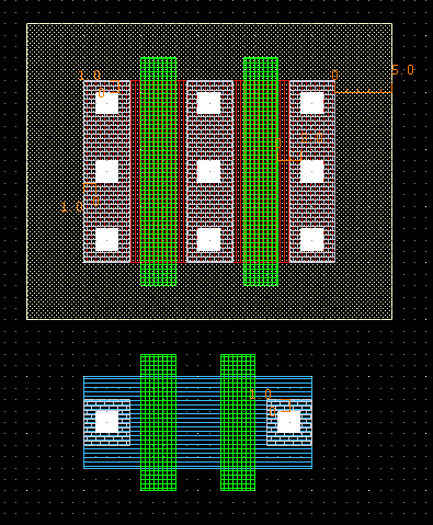
The last step is the interconnect, power bus, and inputs.
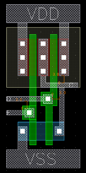
The N-Well space to N-FETs had to be increased to make room for the polysilicon to metal1 connections. This is the layout of a two-input NAND gate.