With a set of design rules to work with, it is now possible to generate actual layout. Remember, all rules must be satisfied.
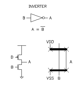
The first step in drawing layout is to determine how large to make the device. Inverters can be many different sizes, so the schematic symbol will indicate the exact size to make the device.
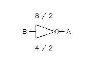
The top number indicates the width and length of the P-FET's channel, and the bottom number indicates the width and length of the N-FET's channel. The channel is under the gate, and is measured in the direction of current flow. Since the current flows from the power node to the output node, the channel width is how tall the gate is, and the length is how wide the gate is. This seems backwards, but remember that the current flows across the FET.
The width and length for the N-FETs is 4/2. This means that the channel width is 4 (how tall the FET is), and the channel length is 2 (how wide the gate is).
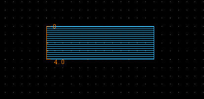
This is a section of N-type diffusion that is 4 microns tall. From the left, we must first add in contacts for the VSS connection.
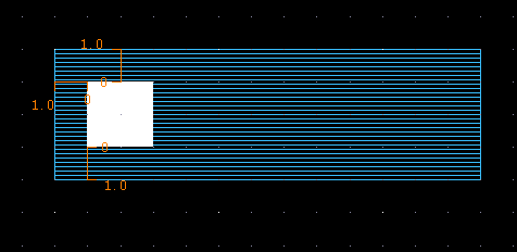
Notice that the N-type diffusion overlaps the contact by 1 micron. Both N-type diffusion and P-type diffusion follow the "active" rules. The contact is also 2 microns square, each contact must be exactly 2 by 2 according to these rules. Now, the polysilicon for the gate must be created.
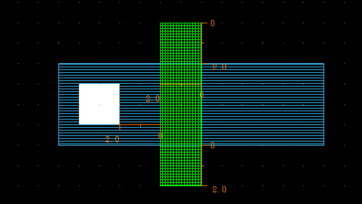
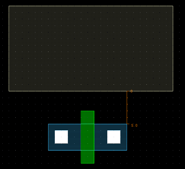
The contact over the active must be 2 microns away from the polysilicon, and the W/L number for the transistor indicated the length of the channel had to be 2 microns long. According to the design rules, the polysilicon endcap must be 2 microns long. The "endcap" is in reference to how much the polysilicon of the gate must overlap the active. Now, the output contact must be created.

The active contact is again 2 microns away from the polysilicon, and the N-type diffusion overlaps the contact by 1 micron. With the N-FET drawn, work can begin on the P-FETs. Since the P-FETs are drawn inside a N-Well, it should be drawn first.
The P-FETs follow the exact same rules as the N-FETs. For an inverter, the FET even looks the exact same except for the change in size.
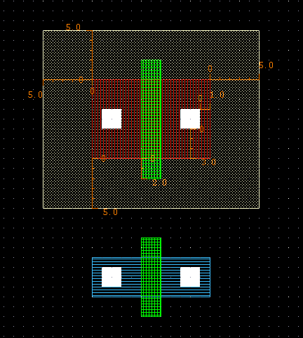
The P-FET is 8 microns tall because the channel had to be 8 microns wide. The P-FET is also enclosed by N-Well by 5 microns. The contacts are placed in the middle of the active to help distribute the current through the device. If the contact was closer to the bottom, most of the current would go through the bottom, and not much would travel through the top portion of the gate.

Metal1 enclosure of contact is 1 micron, and the minimum metal1 space of 3 microns is not violated. The interconnect must also be drawn.

The polysilicon is now connected, and the metal1 output is also connected. The VSS and VDD power connections are a little larger the minimum. It would be logically correct to use minimum width metal. However, it is always a good idea to insure plenty of metal for proper current flow.
At this point, the only thing left is the gate connection, and the power bus.
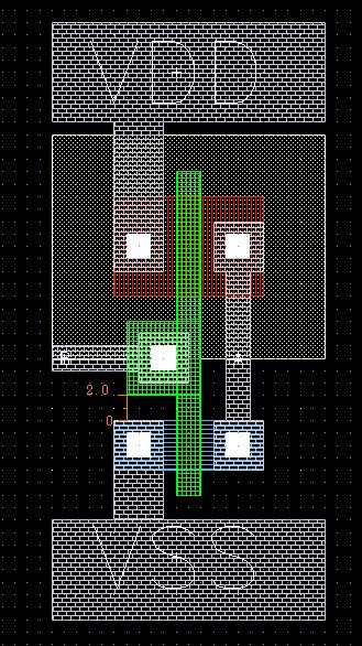
Polysilicon overlap of contact is 2 microns, and the minimum polysilicon space to active is not violated. This is the layout of a basic inverter.