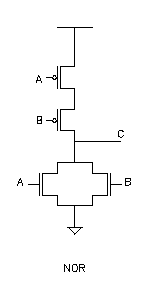
The stick diagram for a 2 input NOR can be worked out in much the same way as a 2 input NAND.
Again, start off with 2 horizontal lines, and one vertical line (that crosses both horizontal lines) for each input. Since there are 2 inputs (A and B), there are 2 vertical lines. This will represent the 4 transistors (2 transistors for each input).
In this example, the gates are named A and B. There is nothing wrong with B and A instead. The stick diagram will just look like a mirror image of what this example will result in.
Now look at the transistor level schematic. For the N-FETs, each gate has VSS on one side and C on the other. This means VSS can be placed in the middle and C on the outside, or C in the middle and VSS on the outside. Again, to keep capacitance on the output down, C should be placed in the middle.
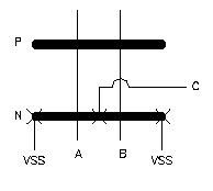
On the other hand, the P-FETs has output C going through B, then A, and finally to VCC. The stick diagram should be set up the same way.
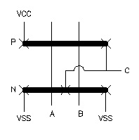
This is the stick diagram for a 2 input NOR gate.
The stick diagram for an INVERTER is very simple, since there is only one input.