Fabrication of Microstructures :
A Non-traditional Technology , LIGA
Caustoobh K Bezboruah
Abstract
:The acronym LIGA comes from the German name for the process (Lithographie, Galvanoformung, Abformung). LIGA uses lithography, electroplating, and moulding processes to produce microstructures of high aspect ratios (~200) with submicron feature sizes, i.e. structures with diameters in the order of a micron and heights ranging from tens of microns to about 2mm. It combines a high degree of freedom in geometry, choice of materials, and potentially low production costs.
1. Introduction
The last decade has seen a tremendous rate of growth and rapid development in microfabrication technology driven by the demand for low-cost microcomponents and microsystems. Application of microsystems have stimulated innovative developments, created new markets and a demand for low cost components.
Micromechanical systems were first produced using the process of wet chemical anisotropic etching of single-crystal silicon . Improvements were made with anisotropic dry-etching by means of plasma or ion beams. The deposition of solid materials by means of dissociation of gaseous chemical compounds in the focus of a laser beam extended the techniques for the production of microstructures. Further developments using x-ray lithography with synchrotron radiation made possible the production of very deep microstructures.
The advantages of deep x-ray lithography over the traditional silicon microengineering techniques are two-fold. One, it meets the need for deep structures particularly where high aspect ratio microstructures are needed with vertical sides. Second, it greatly extends the range of materials that can be used in microengineering other than silicon and related materials, to for example, metals, plastics and ceramics.
The realization of precision deep microstructures requires high-energy, intense parallel beams of x-rays from synchrotron radiation sources and novel processes technology. Because of the short wavelength of x-rays, an extremely high resolution is achievable in a shadow printing process, and in principle, inherent problems with optical lithographic systems which result from the low depth focus of high resolution systems can be avoided. Deep x-ray lithography is basically a shadow printing process in which a two dimensional pattern is accurately transferred from a mask into a resist material by chemical changes induced by the radiation. In the process, as originally developed, the primary template so generated by synchrotron radiation lithography is filled with metal by electrodeposition. The metal structure so produced is used as a mould insert for the fabrication of secondary plastic templates which, in large scale production, take the place of primary plastic templates. This process, known as LIGA(Lithographie,Galvanoformung
and Abformung), first developed in Germany, is based on a combination of lithography, electroforming and replication processes.
Microstructures have been obtained showing high spatial resolution, high aspect ratios, great structural heights, and perfectly parallel edges. With such impressive results there is a lot of interest in LIGA for production of other microstructures as well. Applications for microstructures exist in many sectors of industry. These include chemical and process engineering , biomedical instrumentation, automotive and aerospace technology, environmental monitoring and
information technology. Emphasis is being placed on three main areas, micromechanics, micro-optics and microfluidics, which are emerging with the widest range of industrial applications.
Integrated microsystems technology, known as microelectro-mechanical systems (MEMS), is based on the integration of mechanical components with silicon chip technology. In Europe, the term microsystems technology (MST) is used in the same context. MEMS technologies are established in many countries, particularly in the USA, Japan and Germany.
This paper reviews the basic steps in microfabrication technology using the LIGA process. It includes also applications of such structures, and a brief review of other non-traditional technologies for microfabrication. Most of the information and material are taken from various resources on the internet and also published papers in journals.
2. Basic principles
[3]
The fabrication of microstructures by means of the LIGA method is not restricted to a fixed sequence of exactly specified steps. It is only characterized by the fact that, in the first step, a template of three dimensional microstructure is generated by the deep etch lithography while the following replication steps depend on the specifications of the product. And the deep etch lithography is preferably carried out by synchrotron radiation. For certain applications, even other lithographic methods such as deep UV, high energy electron beam can be used if one does not need high aspect ratios. The subsequent steps usually comprise microelectroforming and micromoulding processes, and if required, other standard microfabrication processes.
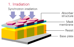
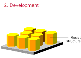
Figure 1 shows the rough process sequence of a typical LIGA process. It should be noted that LIGA is characterized by a large number of possible process steps and materials. The final applied process step depends on the desired product.
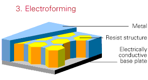
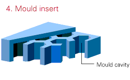
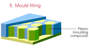
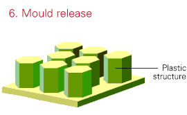
Figure 1.
General process steps in LIGA [6]
An x-ray resist layer is applied to a stable metallic base plate which is irradiated through an x-ray mask with synchrotron radiation. The mask consists of a thin membrane of low atomic weight material with a good transparency for x-rays and an absorbing pattern of high atomic weight material. The irradiated parts of the resist layer are dissolved to obtain a resist structure on the base plate. The next step, involves deposition of metal from an electrolyte, and a metallic structure being built up in the gaps of the resist structure till the metal layer is thick enough. Thus, a stable metallic relief which is complementary to the resist relief is generated. After removal of the resist, the metallic relief serves as a mould insert for subsequent micromoulding processes. This mould insert can be used many times lowering the costs for producing microstructures.
There are numerous possibilities of shape. Conical or pyramid-shaped microstructures can be generated when the angle of incidence of parallel synchrotron radiation is varied relative to the mask and the substrate, i.e. the elements are simultaneously tilted relative to the beam. Structures with different heights can be made by means of multiple irradiation at different wavelengths and penetration depths, respectively. By using composite layers of positive and negative resists,
bridge and cantilever configurations can be realized. Moreover, microstructures can be built up successively by multiple lithographic and electroforming steps where cross-sectional steps are changed in each step. Correspondingly, three dimensional mould inserts can be fabricated and used for a multiple reproduction of complementary microstructures from plastics. The controllable lateral growth of metal on the surface of the resist in the electroforming process can be utilized to fabricate mushroom shaped or even more complex three-dimensional microstructures.
3. Fabrication Issues
[1,2]
3.1 Synchrotron Radiation
The radiation emitted by relativistic electrons when traversing a magnetic field can be explained by classical electromagnetic theory, its properties being explained by the basic equations which are used in the design of synchrotron radiation sources. The power of the emitted radiation is inversely proportional to the mass of the charged particle, so electrons yield useful quantities of radiation in the visible and x-ray regions of the electromagnetic spectrum.
Centripetal acceleration of highly relativistic charged particles in a magnetic bending field results in the tangential emission of synchrotron radiation over a wide spectrum at every point of the curved trajectory. Due to both longitudinal and transverse oscillations of the circulating electrons, individual components in the frequency spectrum become smeared out, resulting in a continuous spectrum of radiation being emitted from the infra-red to wavelengths shorter than a critical wavelength l c in the hard x-ray region. The spectrum shape is characterized by the electron energy, the beam current and the magnetic field in the accelerator.
3.2 X-ray lithography
For dimensions in the submicron range, resist layers of a few micron thickness is sufficient which can be produced in an adequate quality by spinning a liquid resist on the substrate and subsequent baking for solvent removal. As the thickness of the resist is small, relatively soft synchrotron radiation is required (characteristic l c ~2nm)
Irradiation process. Physical and optical constraints on the beam lines from storage rings, such as the distance of the lithography station from the electron beam, beam divergence can have an effect on the beam characteristics delivered at the end station. With respect to fully utilizing the accuracy potential, the local divergency of the synchrotron radiation at the sample must not exceed some 0.1mrad. Filters are used to produce a narrowing of the energy distribution of the beam. An appropriate irradiation process always causes in the horizontal direction a small local divergency. In the vertical direction, however, variations can be averaged out by scanning the mask-resist combination across the beam with a highly accurate beam scanner. Ideally, it should be possible to align, rotate and tilt the mask-resist assembly with respect to the beam.
To utilize the accuracy potential of the technique, it is essential to use a resist and developer system with a ratio of the dissolution rates in the exposed and unexposed areas of approximately 1000. Using poly(methylmethacrylate)(PMMA) as a resist, the minimum x-ray dose for the resist to become soluble in the developer solution (typically, a mixture of glycolic ether, an azine, a primary amine, and water) can be as low as 3kJcm-3 , and a upper limit of 25kJ cm-3 (because of bubbling at the surface due to thermal effects). These define the part of the x-ray spectrum that should be used for a given resist material, its thickness and the thickness of the absorber on the mask.
Figures 2 and 3 show some typical irradiation arrangements.
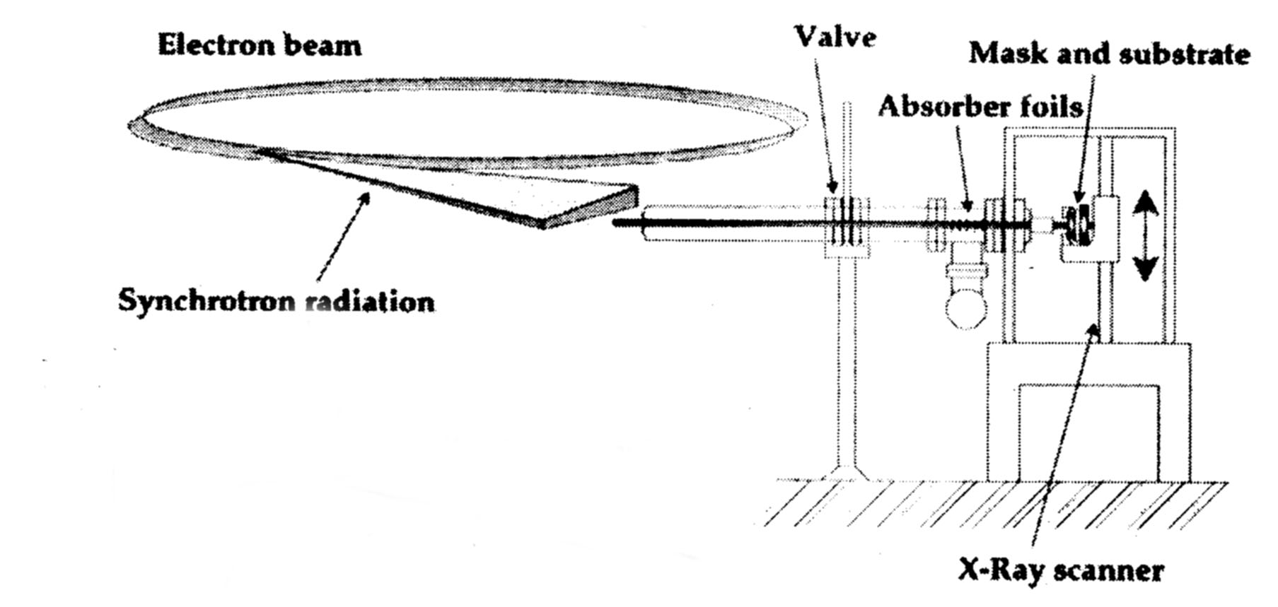
Figure 2. Exposure station for x-ray lithography [1]
Accuracy of pattern replication. The accuracy of the pattern transfer from the mask determines the precision of the microstructures. The accuracy in turn is determined by a number of processes. Two competing processes determining the edge profiles are:
Fresnel diffraction. At the mask absorber edges diffraction effects occur which smear the dose distribution in the resist at the edges of the microstructure. The Fresnel pattern gives the distribution for a monochromatic radiation in the resist as a function of the lateral distance from the absorber edge. The distance of the first maximum xmax form the edge in a depth z in the resist is
![]()
Taking this as a measure of the pattern transfer accuracy, the expression indicates that lateral deviation decreases at shorter wavelengths.
Photoelectrons. The interaction of x-rays with the resist creates photoelectrons in a small volume surrounding the event. For electrons scattered out in the shadow region of the resist, the maximum penetration depth , R is
![]()
In contrast to Fresnel diffraction, a shorter wavelength increases the range of photoelectrons with a corresponding loss of accuracy in the pattern transfer.
The two effects give a minimum of structural deviations when the characteristic wavelength ranges between 0.2 and 0.3nm, which determines the wavelength of the source.
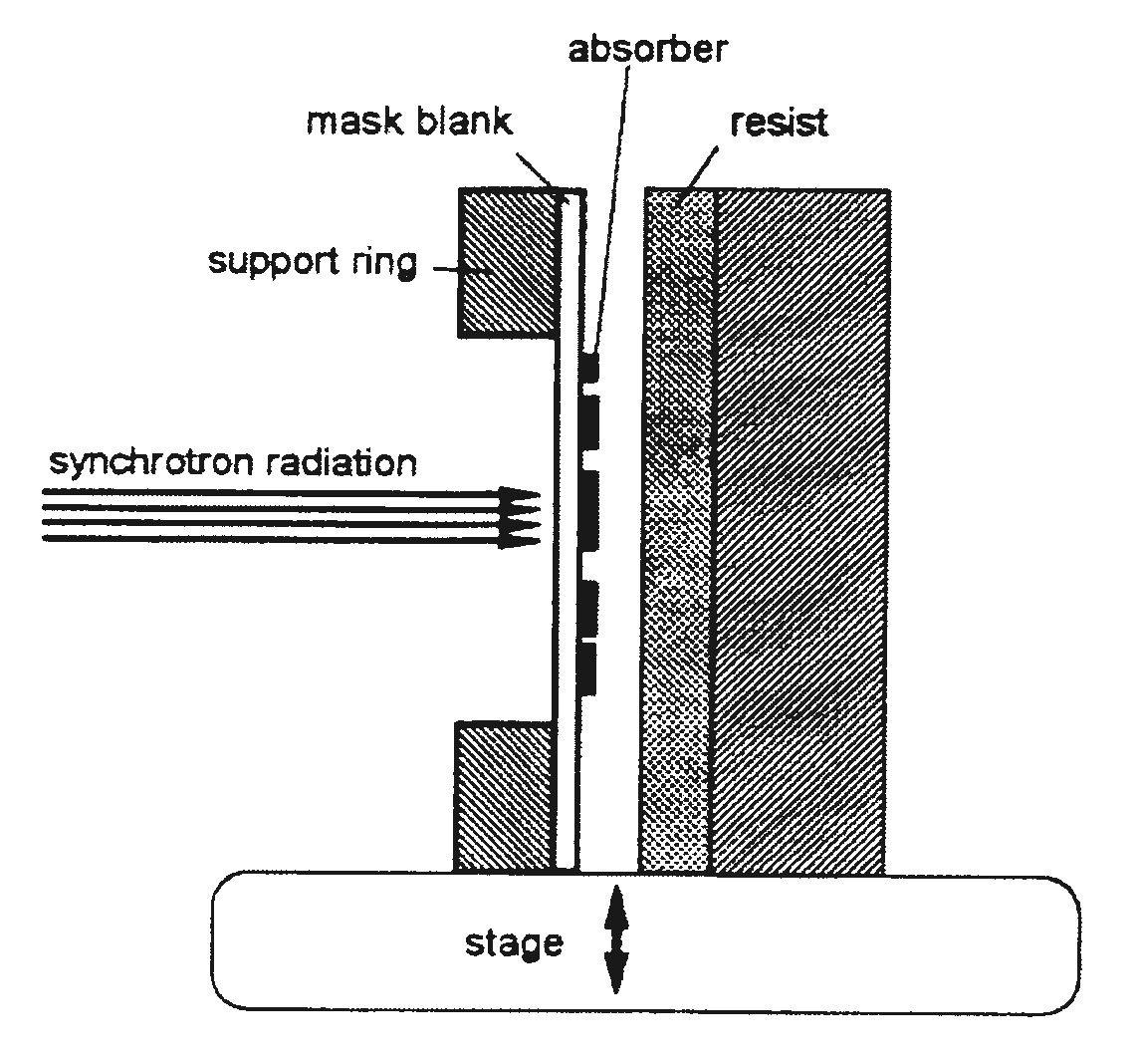
Figure 3. Incident beam on mask-resist surface [1]
3.3 Fabrication of X-ray masks.
Basic requirements. The comparatively short wavelength used in synchrotron radiation lithography within the LIGA process and the high power densities required for a short irradiation time make much greater demands on the masks in terms of transparency of the membrane, its resistance against high irradiation doses, and its contrast than are usually known in the field of synchrotron radiation lithography. The first step is to produce the design of the absorber structure on a thin membrane known as a mask blank. The absorber, a metal layer, must have a high stopping for x-rays and be coated with a viable membrane or mask blank transparent to x-rays. As an ideal mask cannot be fabricated, a compromise is made.
Materials. A distinct contrast between the absorption and transmission for x-rays in the absorber and mask blank is required. In the relevant range only diamond and beryllium are favourable mask blank materials because of their high x-ray transparency and good mechanical properties. Beryllium has the most suitable combination of mechanical and thermal properties, allowing the electroplating of thick absorbing structures onto membranes of low deformation. The necessary absorption of the absorber structures is obtained by application of a 10 to 15 micron thick gold layer on the membrane.
For intermediate masks (lower-energy) silicon carbide, diamond, and silicon membranes are also used. These materials are limited to relatively short periods of irradiation because of thermal instability but their low cost makes them useful for development work.
Fabrication routes. The three different fabrication routes for x-ray masks are illustrated in Fig.4. The characteristics of the synchrotron radiation, the type of resist, the absorber material, the mask membrane and the filters used in the beam to remove its low-energy content have to be taken into account when designing the mask.
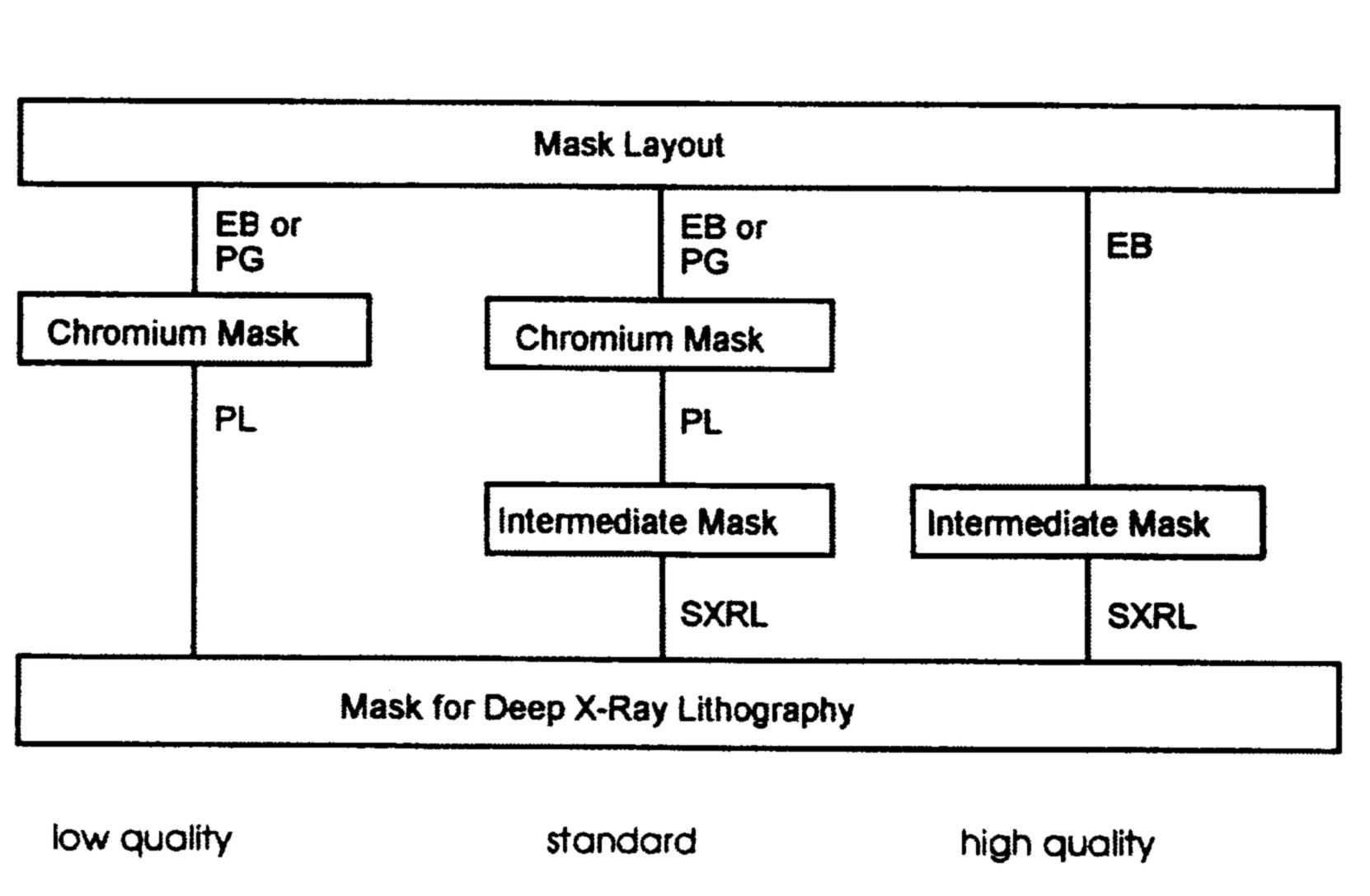
Figure 4. Routes for fabricating x-ray masks [1]
3.4 Resists.
Resists have to be made of materials which have high absorption coefficients at the critical wavelength of the x-rays being used. They have to be produced in the form of films with thicknesses between 100micron and up to 2mm. Resists have to be soluble in a suitable etchant after exposure to x-ray irradiation.
Materials. PMMA has almost become the standard resist material. It is essential that the PMMA is bonded to the metallic substrate in order to proceed with electroforming. The preferred adhesion promoter is trimethoxysilylpropyl methacrylate. A thin layer of titanium is also sputtered to the substrate for better adhesion.
Processing. The developer should dissolve the irradiated parts as uniformly as possible without attacking the unirradiated material. The longer development times required in deep x-ray lithography cause swelling and distortion in the resist and therefore standard developers cannot be used. One recent developer being used is a mixture of ethylene glycole monobutyl ether, monoethanolamine, tetrahydro-1,4-oxazine, and water.
The development of x-ray lithography depends on the development of new resists. Research is being carried out at various centres. The Institute of Microtechnology at Mainz has produced a negative resist 20 times more sensitive than PMMA.
3.5 Results of x-ray lithography.
Figure 5 shows some of the typical structures formed by x-ray lithography.
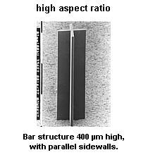
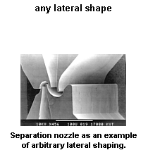
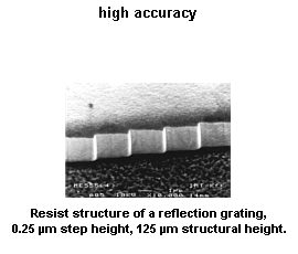
Figure 5. Typical structure fabricated using x-ray lithography [7]
3.6 Galvanoforming (Electroforming)
The fabrication of metallic relief structures by electrodeposition of metals on patterned polymer surfaces is a process long since experienced on a commercial scale. The fabrication of tools for records and video disks where structural details in the submicron range are transferred uses electroforming. In the LIGA process, however, the increase in the aspect ratio of the microstructure by several orders of magnitude, creates new difficulties. Commonly used electroplating materials are metals such as gold, copper and nickel.
The exact processing method for galvanoforming depends on the nature of the microstructures required. A range of techniques are available (Fig 6)
Figure 6. Process and materials for galvanoforming [1]
The processes depend on the surface technologies; the rate of deposition being hydrodynamics and electrolytic processes limited. For producing deep microstructures aqueous solutions of gold, nickel, copper, and nickel-cobalt alloys are used. Deposition times can extend to many days. For non-defective microstructures extremely pure and clean electrolytes are essential.
3.7 Micromoulding.
Micromoulding processes provide the route to mass manufacturing. It is the least developed of the LIGA processes and hence the subject of intense research. The severe aspect ratio requirements create problems here too. Also, the secondary plastic templates produced by moulding do not normally represent the final product, but are to be filled with a metal by electrodeposition as is done with the primary templates produced by the lithographic technique. So, in general, the secondary plastic templates, too, must be provided with an electrode or plating base.
Even high aspect ratio features can be moulded with polymers provided the polymer used as a moulding mass has small adhesive powers and rubber-elastic properties. However, rubber-type plastics by nature have a very low stability of shape which make them unsuitable for moulding of free-standing microstructures having high aspect ratios. Current materials include PMMA, polycarbonate (PC), polymide (PA), polysulfonate (PSU). The polymers must have low viscosities, low stresses and be application matched.
Special injection moulding machines are required since the process places certain restrictions. To ensure that the temperatures are high enough to prevent solidification before all the cavities are full, a molten polymer has to be introduced. Moreover, relatively high temperatures are needed to reduce viscosity of the mould polymer. After injection the temperature is reduced until the material reaches a high mechanical stability to allow separation from the mould insert.
Many industrial applications exist for precision microceramic structures as well. These are produced using slip casting techniques. Products based on alumina, zirconia and piezoelectric (PZT) materials have been used.
4. Other Non-traditional Microfabrication Techniques
[4,5]
In parallel to the evolution of silicon-based and microelectronics derived technologies, other technologies have originated, often in other fields and can also contribute significantly to the development of microsystems, and actually even open new perspectives in this area. The ones discussed briefly here are chosen on the basis of their novelty and prospective width of application.
The first is of course, LIGA already discussed in some detail. There are two variations of LIGA as well.
4.1 Electron beam LIGA
This has the advantage of ?direct write? mode where resist is exposed directly by computer controlled beam without the need for expensive masks. Not only do costs go down but also the
greater precision and flexibility attributes of electron beam machines can be brought to LIGA.
4.2 Microelectro discharge machining (EDM)
Micromachining using electro-discharge makes it possible to achieve precision machining of microholes, micro shafts and a variety of complex shapes. The process is based on the erosion of the material to be machined by means of a controlled electric discharge between an electrode and the material.
The three different machine tools developed for obtaining microholes, microshafts and complex shapes by micro EDM can be conceived as closely corresponding to the ?macro? equivalents like the drilling machine, the lathe and the milling machine respectively. The machinable materials are usually electrically conductive, but semiconductor materials, such as silicon, can also be machined. Hard materials like cemented carbide can be micromachined quite easily.
4.3 Micro stereo lithography
For fabricating real 3D objects with high aspect ratios, particularly when complex microstructures exhibiting curved surfaces must be fabricated, both LIGA and EDM have drawbacks in general. A process based on stereo lithography, named the IH process, and first introduced in 1987 is expected to revolutionize the field.
The basic principle consists of generating a 3D structure, made out of ultraviolet radiation curing polymer, starting from the construction of 2D sliced thin plates hardened from a liquid by UV radiation. The light source typically is a He-Cd laser or a xenon lamp; the beam is controlled by a XYZ-stage in order to draw a 2D shape directly from a CAD system. The polymeric structure so fabricated can be directly used as a microcomponent, or as a cast for a metal moulding process for obtaining 3D structures. Microstructures that can be fabricated include polymeric curved micropipes with square cross-sections, polymeric cell microsprings, one way microvalves.
4.4 Hybrid microstructures
For applications in the development of artificial organs, biosensors, or biochips usable as computer elements, hybrid structures which integrate biological and artificial materials, are very attractive. In addition to technologies and tools for fabricating nanostructures by handling individual molecules and even atoms, one intriguing area is that of ?intelligent materials?.
The approach is based on the concept that materials can be ?tailored? in order to incorporate
many different functions in addition to the structural ones, specially the ability to ?adapt? their properties to external events. That is, they possess sensing, processing and actuating functions. This typically biological behaviour if imitated by artificial structures can give ?biomimetic? structures.
An example of an intelligent structure usable as a microsystem or a micromachine component are the chemical sensors. A possible fabrication approach for such biomimetic materials is to build materials with components that dictate their own assembly and their assembly provides the material with specific features. One powerful technique is the Langmuir-Blodgett technique (ref)
There are a variety of techniques and interdisciplinary efforts in this area. Hybrid technologies can provide almost all components of micro and nano devices. The mechanical structure of the microsystem can be fabricated by microfabrication, and using different materials followed by integrating the ?biocomponents? into it.
5. Applications of the LIGA Process
[1,3]
The various advantages, particularly, the high precision, aspect ratio and structural height, the unrestricted design in the cross-sectional shape, the wide variety of materials and the potentiality for achieving low costs in mass production, have resulted in a large application potential for LIGA. The three main application areas are : micromechanics, micro-optics and microfluidics.
5.1 Communication technology
Micro-optics, particularly today when glass fibres are being used for high speed transmission, is a key area in communication technology. Micro-optic components include switches, waveguides, multiplexers, zone plates, monomode fibre connectors and mechanical alignment systems, and nozzle plates for ink-jet printers.
5.2 Optical components
These include microsensors, microconnectors, mounts, supports and packaging and optical-fibre alignment systems. In the field of sensors, we can have micro-optical elements like waveguides,
gratings, couplers, mirrors, spectral filters as well as complete systems like miniaturized photomultipliers with multiple dynode arrays and simultaneous spectrometers. Since a number of transparent polymeric materials like PMMA and flourinated poly(butylmethacrylate) can be used as x-ray resists, optical microstructures can be fabricated directly by x-ray lithography. By using multiple layers of such materials with different refractive indices, slab waveguide structures can be generated.
5.3 Photonic band gap structures
The optical properties of dielectrics can be altered by spatial microscopic structurization. In structures with a periodically modulated dielectric function, the propagating electromagnetic wave is organized in photonic bands. Electromagnetic radiation can be prohibited by changing the dielectric constant of the material enabling it to be used as a filter. There are a number of proposed applications for photonic band gap structures with operating frequencies in the microwave to optical region, such as mobile communications networks, millimetre wave components as planar antennas, millimetre wave oscillators and threshold lasers.
5.4 Automotive technology
The automotive sector of industry uses one of the largest volumes of microproducts, mainly sensor-based for the measurement of pressure, acceleration and control of air bags, active suspension systems, engine monitoring and safety systems. Also included are microinjectors and micronozzles for efficient fuel injection systems, immobilizers, antiskid and vision enhancement systems.
Sensors for measuring vibration or acceleration consist of a mechanical system with a spring and a mechanical mass. For measuring position, displacement, small distances or magnetic fields, sensor devices with inductive elements are applied.
5.5 Chemical and biotechnology
Miniature modular chemical process plants and monitoring systems could offer low-cost solutions for environmentally acceptable chemical processing. Components being developed include microfilters, micropumps, micro-actuators, microreactors, chemical mixers, novel sensors and microfluidic systems.
Microstructures in the field of fluid technology is a fast growing field with devices such as microvalves with extremely short response time, novel columns for chromatography, microcooling systems based on the Joule-Thompson effect, miniaturized heat exchangers with high efficiency, nozzle arrays for inkjet systems, fluidic circuits, novel spinneret plates for synthetic fibre production and continuous flow microreactors.
Miniaturized total analysis systems are being used with very small samples based on the Lab-on-a-Chip concept, which have applications in monitoring and biomedical diagnostics. Biochemical sensors integrated into miniaturized measurement systems are another thrust area.
5.6 Medical technology
The requirements for microcomponents and microsystems in medical technology is very diverse, extensive and wide ranged. Major thrust is in the field of drug delivery, in vitro diagnosis, monitoring and minimal invasive surgery(MIS).
Relevant microproducts are high resolution, dextrous grippers, micromanipulators, transducers and sensors for MIS, drug delivery and implants. Microrobotics and miniature rotors driven by microturbines can be used for a number of surgical applications.
The use of ultrasound imaging techniques can be significantly improved by using a micromotor mediated movement of the catheter tip to reduce image distortion. Implantable micropumps are used in drug delivery systems where small amounts of a precise drug dose have to be administered over a long period of time, as in diabetes treatment.
5.7 Composite and carrier microstructures
Composite materials fabricated by methods like reinforcement by fibres or sintering of components result in an irregular microscopic distribution of materials, and hence, a random local variation of material properties might occur. In contrast, LIGA allows production of completely regular layers and plates of composite or carrier materials, where the microstructures in the material can be designed according to its specific application.
6. Conclusions
The LIGA method using deep-etch x-ray lithography in combination with electroforming and moulding is not only a promising tool for fabricating a wide variety of microstructures products but also has reached an advanced stage where most of them are realizable.
The increasing trend of miniaturization will put much demands on the method and it is felt that there is an urgent need to establish a manufacturing methodology underpinned by a research and development base.
The manufacture of microstructures with full three-dimensionality in geometry and function would require new design tools. Microcomponents would have to be microengineered into system to be useful. Computer-based design tools, including 3D modelling and simulation techniques need to be employed.
Key technological areas are believed to be : improving pattern resolution from micron to submicron levels, enhancing the submicron precision lengths from millimetres to centimetres, reducing the irradiation time through the use of improved resists and hence the cost of x-ray lithography from hours to minutes, and the establishment of industrial standards for materials, dimensions, equipment and reliability.
Finally, of course, markets will be the drivers for improved and new process technology but it is believed that technological and market roadblocks have to be removed before full commercialization of microsystems takes place.
References
This paper has been based on material from the following among others :
1. Tolfree D W L , Rep. Prog. Phys. 61 (1998), 313-351
2. Becker E W et al , Microelec. Eng. 4 (1986), 35-56
3. Ehrfeld W et al , Nucl. Instr. Meth. Phys. Res. A 303 (1991), 523-531
4. Dario P et al , Jr. Micromech. Microeng. 5 (1995), 64-71
5. Lawes R A , Sensor Rev. 16 (2), 16-22
6. http://www.imm-mainz.de/ The web site for IMM, University of Mainz, Germany
7. http://www.fzk.de/imt/ The web site for the Institute of Microstructure Technology, Germany where LIGA was initiated