
|
| Costel Rizescu |
|
RADIATION DETECTORS |
RADIATION DETECTOR: What it is, what it does?
SCINTILLATORS
Bismuth Germanate - Bi4Ge3O12| Scintillator (Activator) | CsI(Tl) | CsI(Na) | CsI(undoped) |
| Density [g/cm3 | 4.51 | 4.51 | 4.51 |
| Hygroscopic | slightly | yes | slightly |
| Emission wavelength max [nm] | 550 | 420 | 315 |
| Lower Cut-off [nm] | 320 | 300 | 260 |
| Refractive index @ emission max | 1.79 | 1.84 | 1.95 |
| Primary decay time [µsec] | 1.0 | 0.63 | 0.016 |
| Light yield [photons/MeV ] | 52- 56 x103 | 38-44x103 | 2x10³ |
| PMT Photocathode yield [% of NaI(Tl)] | 45% | 85% | 4% - 6% |
Converting gamma -ray energy to electronic charge
Quantum
Efficiency for a
photo-diode is the number of electron - hole pairs that can be detected as a
photo-current divided by the number of incident photons. This is usually
expressed as a "percent" (at a particular wavelength) and is given by the
following relationship:
QE(lambda) = S(lambda) ÷ (lambda) x 1240 x
100%
Where S is the photo sensitivity in A/W at a
particular wavelength, and (lambda) is the wavelength expressed in nm
(nanometers).
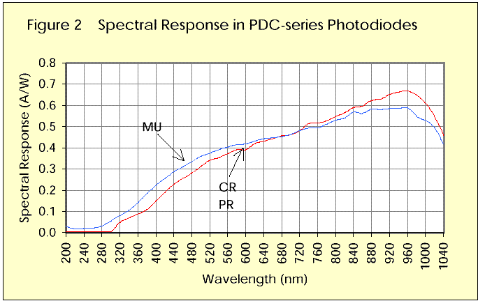
Example 1: In the figure above, the quantum
efficiency of a PDC-series diode with a resin window coupled to a CsI(Tl)
scintillation crystal whose spectral peak is centered at 550 nanometers is the
spectral sensitivity at 550 nm (~0.37 A/W) ÷ 550 x 1240 or ~83%.
Pulse Mode readout using CsI(Tl)
Choice of Diode: In general, pulse-mode read-out requires the use of a back-biased PIN type of photodiode (PDC series) which has a much lower junction capacitance for a given active area, and consequently a much faster signal response, compared with that of a planar photo-diode (PDA series) of the same active area.
Optical Coupling: Since the index of refraction of most scintillation crystals is substantially higher than 1.0 (1.0 is the index for air and is close to the value for the resin window on a Si diode), getting the scintillation light out of the crystal and into the diode almost always requires the use of an optical coupling medium - a gel or silicone grease for temporary construction, or an epoxy-based compound or other resin-type adhesive for permanent construction.
For optimum light-transmission, the coupling medium should have an index of refraction which is the geometric mean (i.e., the square root of the product) of the indices for the crystal and the entrance window of the diode.
Determining the efficiency of optical coupling in a scintillation detector: One can estimate the optical coupling efficiency between crystal and photodiode using a small (~1 uCi) low-energy gamma-emitting check-source, such as 241Am (59.5 KeV principal gamma emission). This is about the maximum useful energy for this technique, since detection efficiency in a Si photodiode drops very quickly at higher photon energies, and detection in the scintillator crystal begins to swamp the the overall system count-rate.
Assuming the detector assembly is not completely opaque to the 59.5 KeV gamma rays, one can position the source on the rear (diode side) of the detector so that some of the incident radiation is detected directly in the PIN photodiode, rather than in the crystal. The results of one such experiment are shown below. The detection efficiency for 59.5 KeV gamma rays in Si is rather low (~1%), and the attenuation of 59.5 KeV gamma rays by the detector assembly itself is rather high, so these measurements took a few hours to acquire.
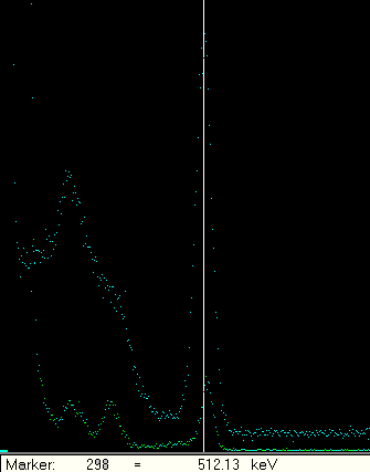
In the figure above, the top-most spectrum is from a 22Na source detected in a 1 cm3 CsI(Tl) scintillating crystal coupled to a 1 cm2 Si PIN diode. The prominent peak is at 511 KeV. The lower spectrum shows a partial gamma ray spectrum from 241 Am detected directly in the Si photodiode, where all of the system parameters, gains, etc., are unchanged from one measurement to the next.
The 511 KeV peak in CsI(Tl) corresponds to channel 297; the 59.5 KeV peak in Si corresponds to channel 302. We know from our data on CsI(Tl) that the conversion from gamma ray energy to optical photons is ~55,000 photons per (absorbed) MeV, or 28,105 photons at 511 KeV. We also know that it requires 3.6 eV to produce one charge-pair (electron-hole pair) for direct detection in Si. Based on the latter measurement we have an absolute measure of electronic charge versus channel number: 59.5 KeV corresponds to 59,500 ÷3.6 = 16,528 electron-hole pairs, or 2.644 x 10⁻¹⁵ coulombs which, in turn, corresponds to channel 302.
The peak at channel 297 from 511 KeV in CsI(Tl) corresponds to a slightly lower value -- 2.6 x 10⁻¹⁵ coulombs. We started with 28,105 optical photons, and the quantum efficiency of our photodiode is ~83%, so if the optical coupling efficiency were perfect we would expect an electronic pulse of 0.83 x 28,105 = 23,327 charge-pairs, or 3.73 x 10⁻¹⁵ coulombs.
However, our 511 KeV scintillation peak turns out to be only ~70% of this value, so we must conclude that the overall optical coupling efficiency for this detector is only ~70%, leaving some room for improvement.
CdZnTe Detectors
CdZnTe radiation detectors were first developed around the beginning of the 1990s. The compound is based on the well known material CdTe, but a fraction of the Cd (Z=48) content is replaced with Zn (Z=30). This yields an increase in the resistivity of the material, reducing leakage current in the detectors and allowing the use of simple planar devices with non-blocking contacts. It also removes the requirement for compensation mechanisms (e.g. Cl doping) often employed in CdTe.
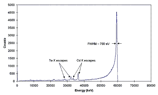
Like many other compound semiconductor materials, hole transport is a major limitation on device operation. The room temperature CdZnTe spectrum below illustrates the effect of hole trapping on photopeak shape. Also visible are the escape peaks of the Cd and Te.
Cooled Detector Results
Cooling to -40 degrees C has lowered the electronic noise to less than 200eV, allowing X-rays to be detected down to 1740 eV (silicon K). Most measurements have been acquired using radioactice sources. A typical Fe-55 spectrum is shown in the figure below. Photopeak resolution is about 238 eV FWHM. The best resolution achieved at this energy is 220 eV. Noise is presently limited by acoustic pick-up. Present packaging limitations prevent complete removal of these effects. Noise analysis shows that 1/f is a dominant noise component, probably contributing > 100 eV to the peak width.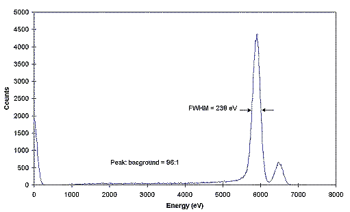

|
CURRICULUM VITAE PUBLICATIONS R & D / Paper ABSTRACTS Manufacturing & Technology HOME |
| Copyright 2004, All rights reserved |